Organic thin film transistor with contact hole and method for fabricating the same

a thin film transistor and contact hole technology, applied in the field of transistor devices, can solve the problems of limiting the application of otft a great deal

Inactive Publication Date: 2007-03-15
IND TECH RES INST
View PDF12 Cites 3 Cited by
  • Summary
  • Abstract
  • Description
  • Claims
  • Application Information

AI Technical Summary

Benefits of technology

[0006] The present invention provides an organic thin film transistor (OTFT) device with a contact hole therein in a simple way, whe

Problems solved by technology

Moreover, the organic semiconductor layer in the OTFT is also easily damaged while being etched, and hence it still

Method used


Image

  • Organic thin film transistor with contact hole and method for fabricating the same
  • Organic thin film transistor with contact hole and method for fabricating the same
  • Organic thin film transistor with contact hole and method for fabricating the same

Examples


Embodiment Construction

[0033] The present invention will now be described more specifically with reference to the following embodiments. It is to be noted that the following descriptions of preferred embodiments of this invention are presented herein for purpose of illustration and description only; it is not intended to be exhaustive or to be limited to the precise form disclosed.

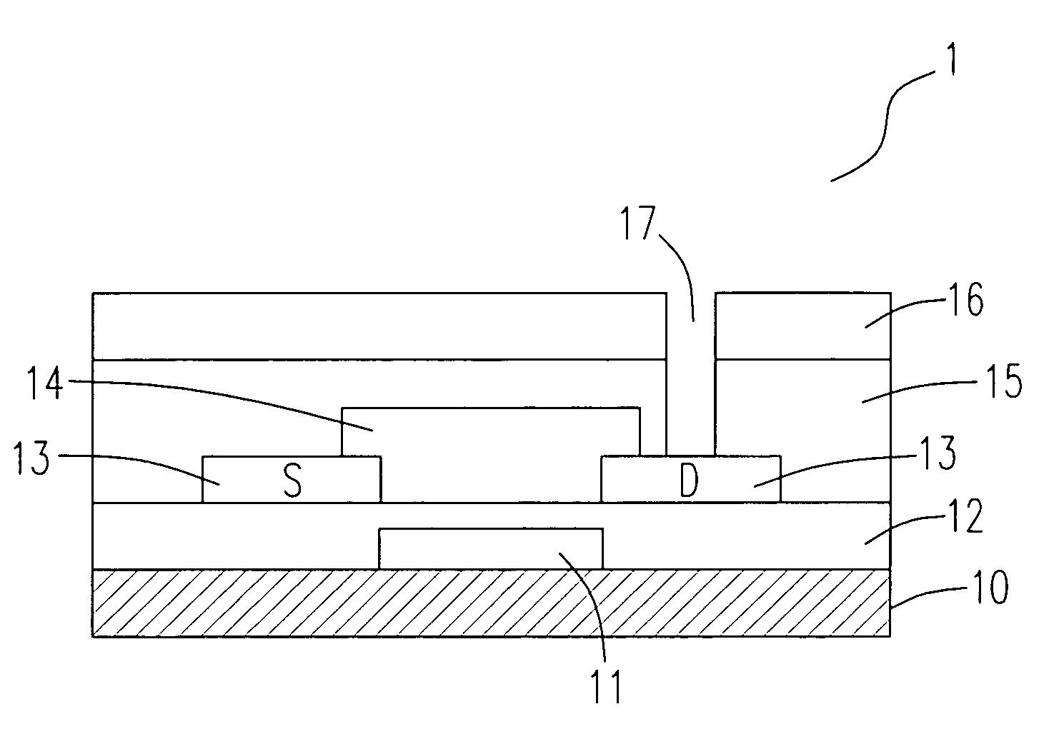
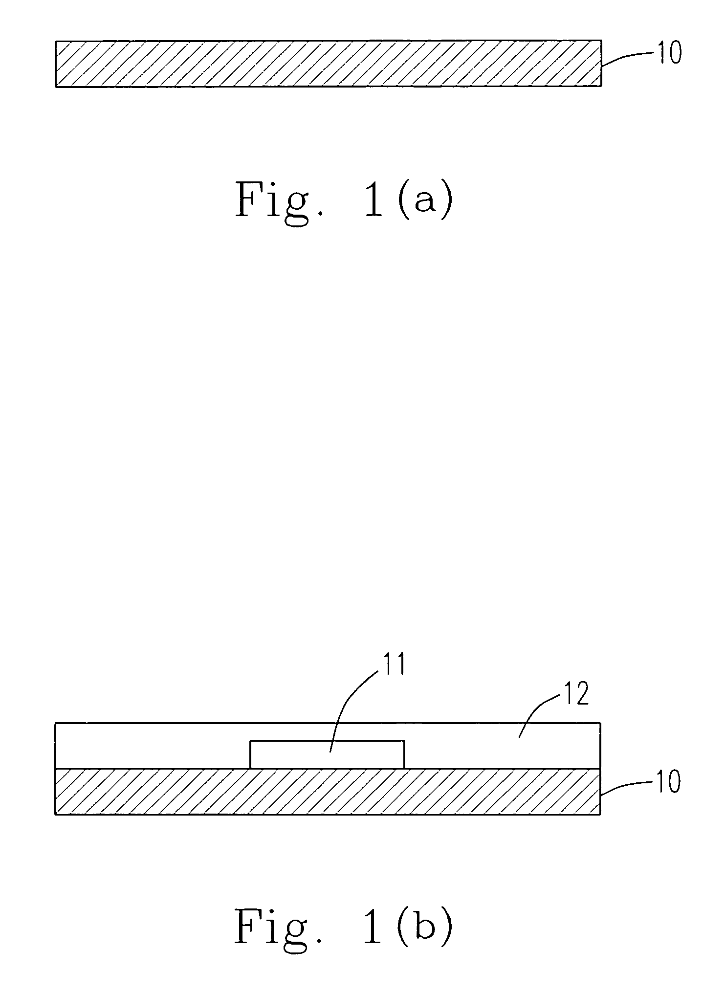
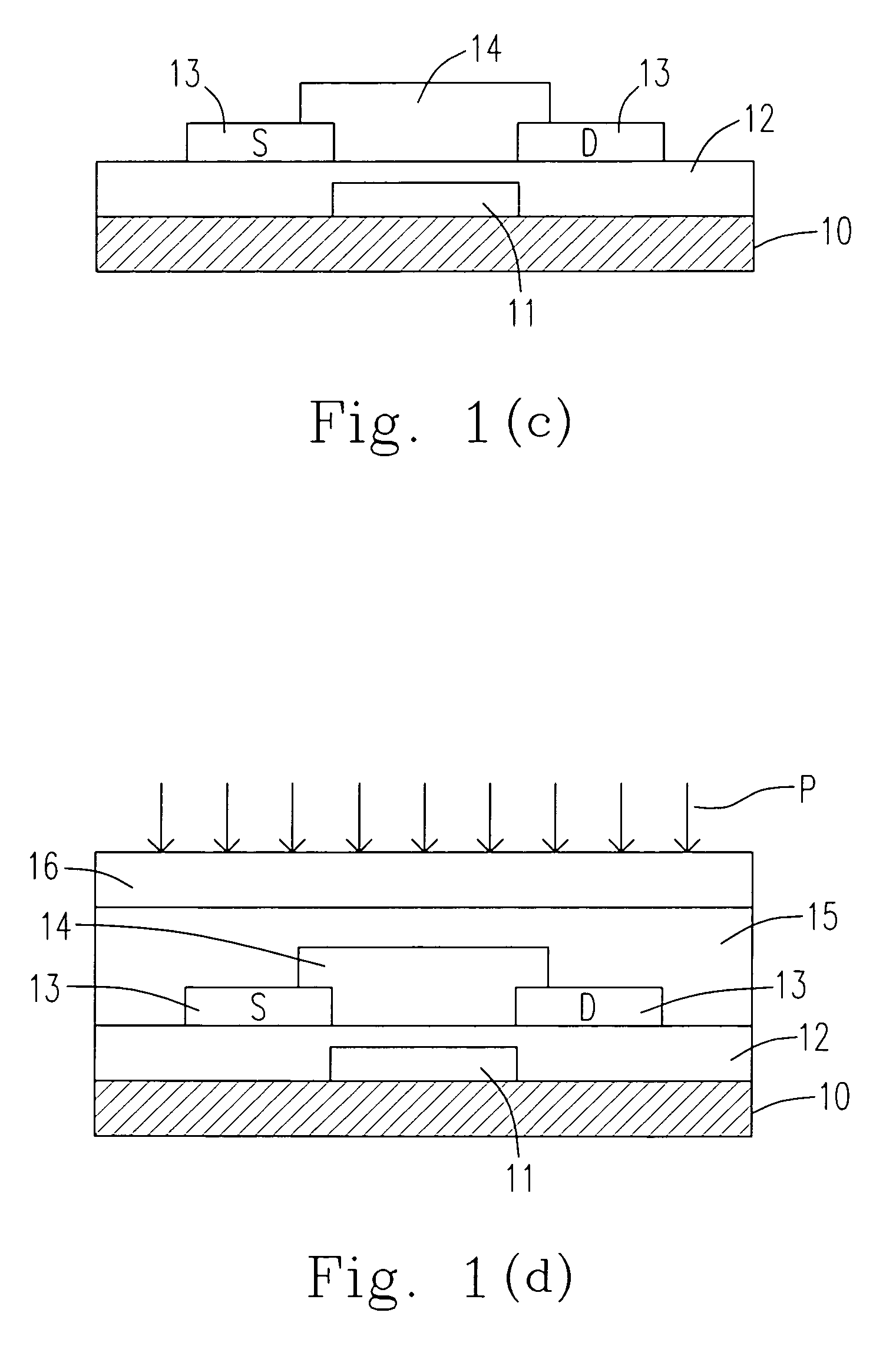
[0034] Please refer to FIGS. 1(a) to 1(e), which are diagrams schematically illustrating the steps of the method for fabricating the organic thin film transistor (OTFT) according to a first preferred embodiment of the present invention and the OTFT having a contact hole fabricated thereby. First, a substrate 10 is provided and a gate layer 11 is formed thereon. The substrate 10 is preferably one of a silicon substrate, a glass substrate, a metal substrate and a plastic substrate. The gate layer 11 forms the gate region of the OTFT device, and thereon an insulating layer 12 is formed. The insulating layer 12 is formed on the gat...


PUM


Abstract

The present invention provides a method for fabricating an organic thin film transistor (OTFT) device where a vertical contact hole is produced in the insulating layer and the passivation layer thereof, so that the respective devices located below and above the OTFT would be electrically connected with each other. The provided OTFT device includes a substrate, a gate layer located on the substrate, an insulating layer located on the gate layer, an electrode layer located on the insulating layer and having a source region and a drain region, an organic semiconductor layer located between the source region and the drain region, a passivation layer patterned and located on the source region, the drain region and the organic semiconductor layer, and a contact hole passing through the passivation layer to one of the source region and the drain region.

Description

FIELD OF THE INVENTION [0001] The present invention relates to a transistor device and the fabrication method therefor, and more particularly, to an organic thin film transistor device and a corresponding method for fabricating the same. BACKGROUND OF THE INVENTION [0002] The organic thin film transistor (OTFT) is now broadly applied for the flexible substrate, the display and the portable electronic device such as electronic tags and intelligent cards, owing to the advantages of simple fabrication and low cost thereof. [0003] Recently, the combination of OTFT and soft electronic device is typically developed in the electronics relevant industry. In particular, it is believed that the improvement of organic transistor plays an important role in the application of OTFT for the flexible display, and more and more efforts are made therefor. [0004] In comparison with the inorganic semiconductor transistor, the OTFT is provided with an organic semiconductor layer, and thus possesses a re...

Claims


Application Information

Patent Timeline
IPC IPC(8): H01L29/08H01L29/04
CPCH01L51/0017H01L51/102H01L51/0545H01L51/0021H10K71/231H10K71/60H10K10/82H10K10/466
Inventor HSIEH, CHENG-CHUNGHU, TARNG-SHIANGHO, JIA-CHONGHSIAO, MING-CHUN
Owner IND TECH RES INST
Why Eureka
Try Eureka