LCD source driver for improving electrostatic discharge

a source driver and electrostatic discharge technology, applied in the direction of semiconductor devices, semiconductor/solid-state device details, electrical apparatus, etc., can solve the problems of poor esd performance poor esd performance, etc., and achieve the effect of improving the esd performance of the lcd source driver

Inactive Publication Date: 2007-03-15
ELAN MICROELECTRONICS CORPORATION
View PDF1 Cites 11 Cited by
  • Summary
  • Abstract
  • Description
  • Claims
  • Application Information

AI Technical Summary

Benefits of technology

[0005] An object of the present invention is to improve the ESD performance of an LCD source driver not by increasing the chip area.
[0007] Since the wire electrically connected between the output pad and the power-rail ESD clamp circuit penetrates the device are through the path, it is much shorter than that in the case of extending along with the edge of the device area. As a result, the ESD performance of the LCD source driver is improved.

Problems solved by technology

However, the arrangement of power-rail ESD clamp circuits is always limited by the layout of integrated circuit.
Namely, the power wires and the ground wires 18 for the middle output pads 14 are much longer, causing poor ESD performance.
If the chip is still designed as the conventional manner, the ESD performance will be worse and worse.

Method used


Image

  • LCD source driver for improving electrostatic discharge
  • LCD source driver for improving electrostatic discharge
  • LCD source driver for improving electrostatic discharge

Examples


first embodiment

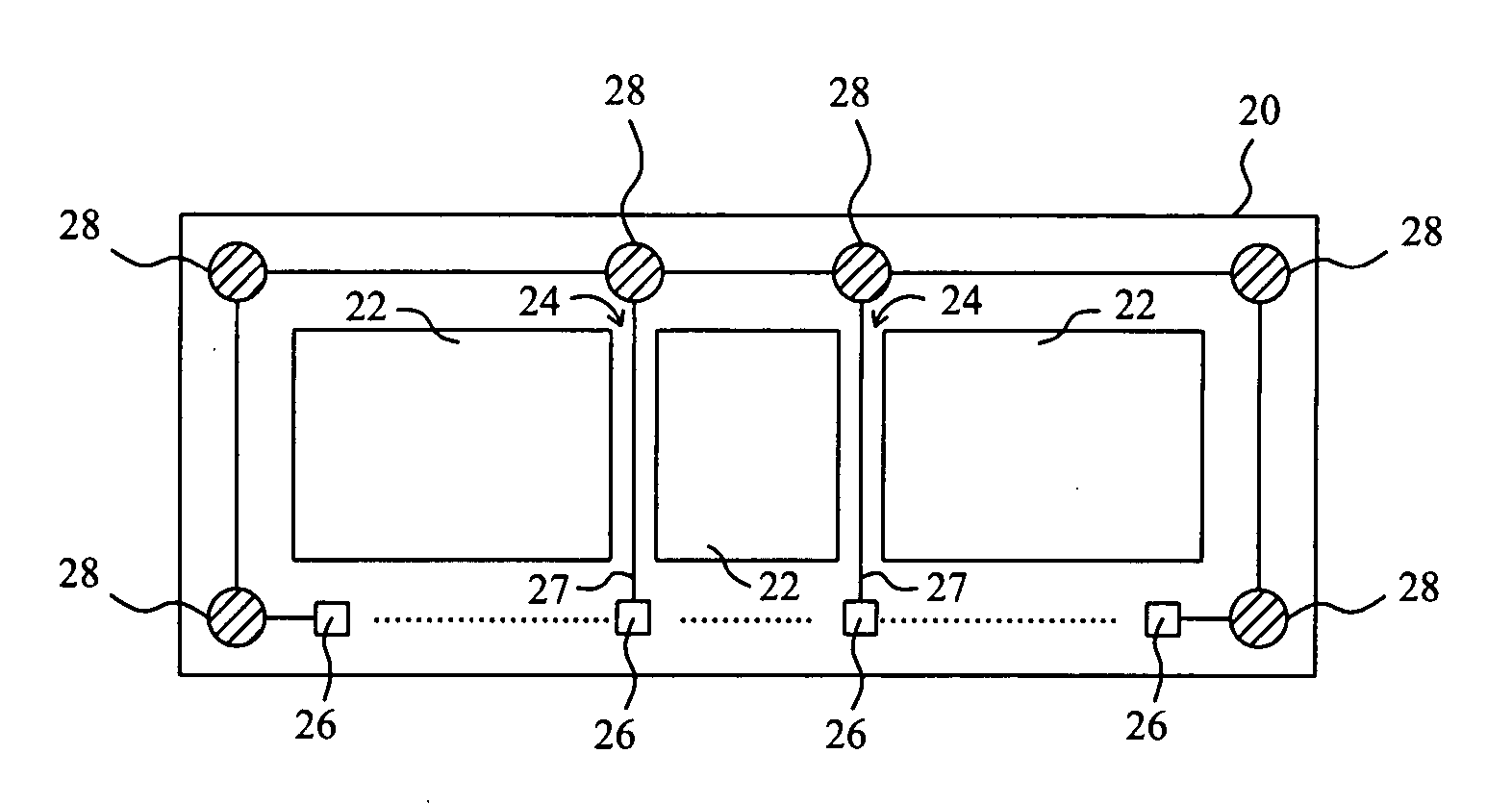
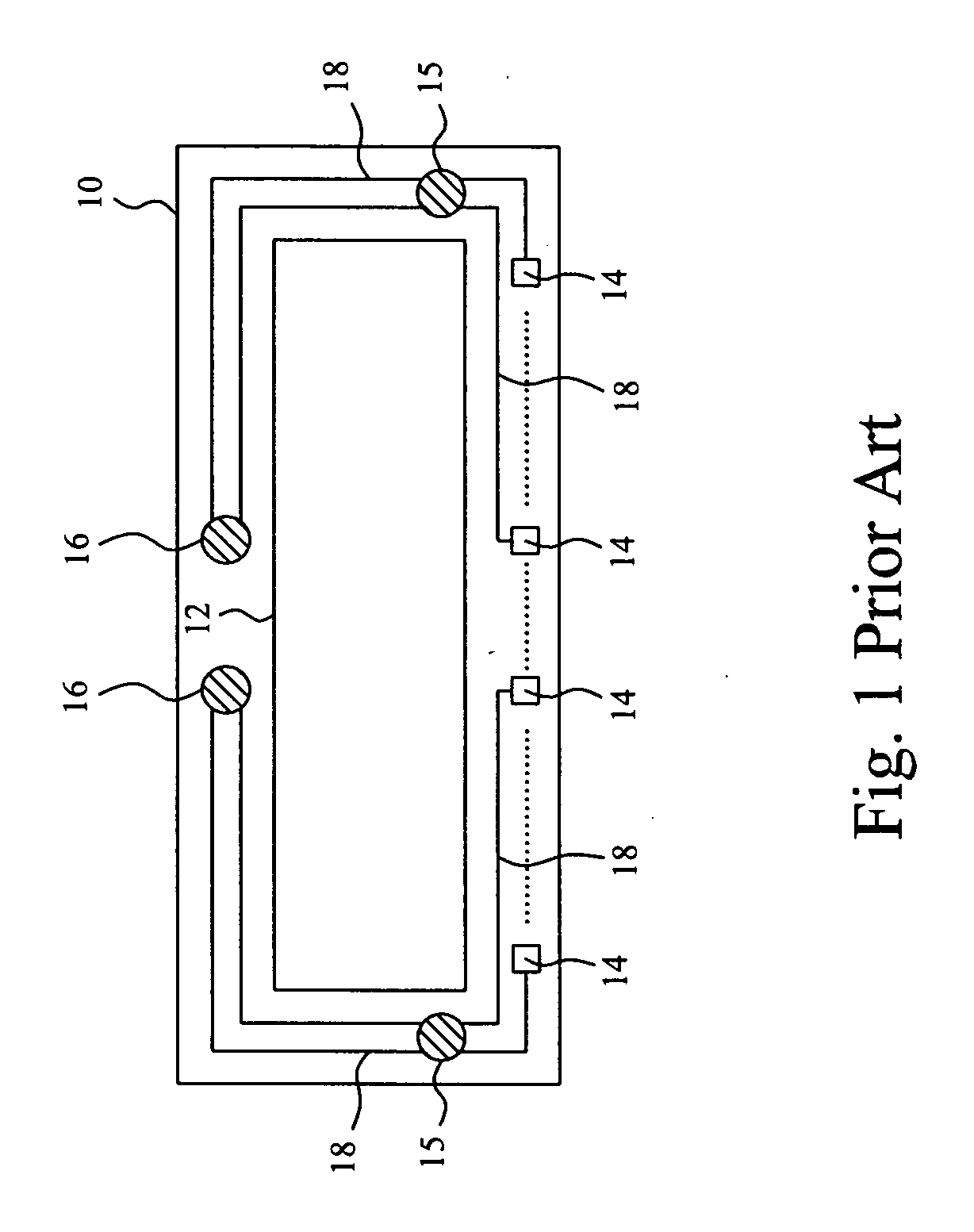
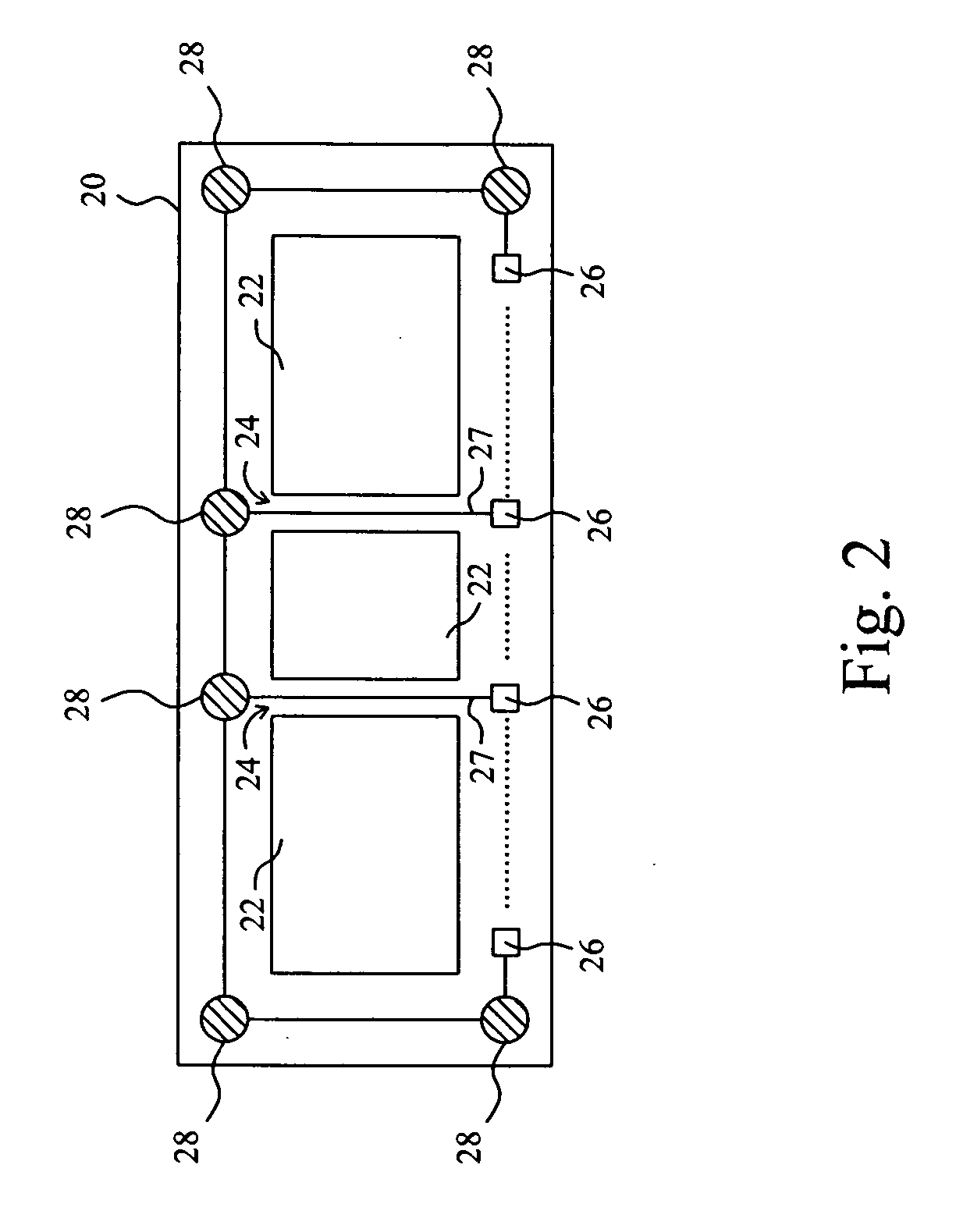
[0013]FIG. 2 shows the present invention. In an LCD source driver 20, a device area 22 has two straight paths 24 thereof, power wires or ground wires 27 for output pads 26 around the middle of the long margin of the LCD source driver 20 extend through the paths 24 to electrically connect to the power-rail ESD clamp circuits 28 on the opposite long margin. The LCD source driver 20 shown in FIG. 2 is a simplified schematic diagram without showing the real scaled size which usually has a ratio of long margin to short margin about 13-17:1. With the paths 24, the output pads 26 nearby the middle of the long margin can directly connect to the power-rail ESD clamp circuits 28 on the opposite long margin through the paths 24, without extending around the whole device area 22, and the power wires or the ground wires 27 are much shorter. Therefore, the ESD performance is improved without widening the power wires or the ground wires 27, or enlarging the power-rail ESD clamp circuits 28. In oth...

second embodiment

[0014]FIG. 3 shows the present invention, in which the paths 24 are not in the direction vertically to the long margin of the LCD source driver 20. One of the paths 24 extends from the long margin where the output pads 26 are to the opposite one in a slant angle, and the other slantwise extends from the long margin where the output pads 26 are to a short margin.

third embodiment

[0015]FIG. 4 shows the present invention, in which the paths 24 crookedly extend from the long margin where the output pads 26 are to the opposite one.

[0016] In other embodiments, no matter how many paths 24 are in the device area 22 or what shape they are, if the path 24 extends from a long margin to another one or to a short margin for internal power wire or internal ground wire, it is always within the scope of the present invention.


PUM


Abstract

In an LCD source driver, to enhance the ESD performance thereof, there is provided a path in a device area penetrating thereacross such that an internal power wire or an internal ground wire to connect between an output pad and a power-rail ESD clamp circuit on two margins, respectively, of the LCD source driver could pass through the path to shorten the internal power wire or the internal ground wire and thereby to avoid chip area increase for the ESD mechanism.

Description

FIELD OF THE INVENTION [0001] The present invention is related generally to a source driver for liquid crystal display (LCD) and, more particularly, to an LCD source driver having improved electrostatic discharge (ESD) protection. BACKGROUND OF THE INVENTION [0002] For ESD enhancement each integrated circuit are not only provided with protection circuits to the I / O pads on the chip, but also inserted with power-rail ESD clamp circuits between the internal power wires and the internal ground wires thereof. Typically, for better ESD performance, the power-rail ESD clamp circuits are prepared at every distance of the internal wires. The shorter or the wider the internal power wire or the internal ground wire is, the better the ESD performance is. [0003] However, the arrangement of power-rail ESD clamp circuits is always limited by the layout of integrated circuit. As shown in FIG. 1, an LCD source driver 10 has a rectangular top plane, and for plenty of output channels, there is always...

Claims


Application Information

Patent Timeline
Patent Type & Authority Applications(United States)
IPC IPC(8): H01L23/62
CPCH01L23/5286H01L23/585H01L23/60H01L2924/0002H01L2924/00
Inventor CHEN, YI-CHAN
Owner ELAN MICROELECTRONICS CORPORATION
Why Eureka
Try Eureka