IO circuit used for enhancing ESD performance

An ESD protection and circuit technology, applied in the direction of logic circuit coupling/interface, circuit, logic circuit connection/interface layout using field effect transistors, etc., can solve the problem of large area occupied by ESD protection devices, limited ESD level, and increased circuit area and other problems, to achieve the effect of improving ESD level, avoiding device breakdown, and reducing circuit area

Active Publication Date: 2015-11-11
CHIPSEA TECH SHENZHEN CO LTD
View PDF5 Cites 2 Cited by
  • Summary
  • Abstract
  • Description
  • Claims
  • Application Information

AI Technical Summary

Problems solved by technology

However, although this circuit protects the ESD circuit itself through the primary protection circuit and the secondary protection circuit, due to the breakdown of the device involved, the trigger voltage is very high, and the ESD level that can be achieved is limited.
There is a risk of breakdown and poor reliability
When the ESD requirements are high, the area occupied by the ESD protection device is relatively large; further, when the driving capability is required, additional driving devices are required, which greatly increases the circuit area

Method used


Image

  • IO circuit used for enhancing ESD performance

Examples


Embodiment Construction

[0017] In order to make the object, technical solution and advantages of the present invention clearer, the present invention will be further described in detail below in conjunction with the accompanying drawings and embodiments. It should be understood that the specific embodiments described here are only used to explain the present invention, not to limit the present invention.

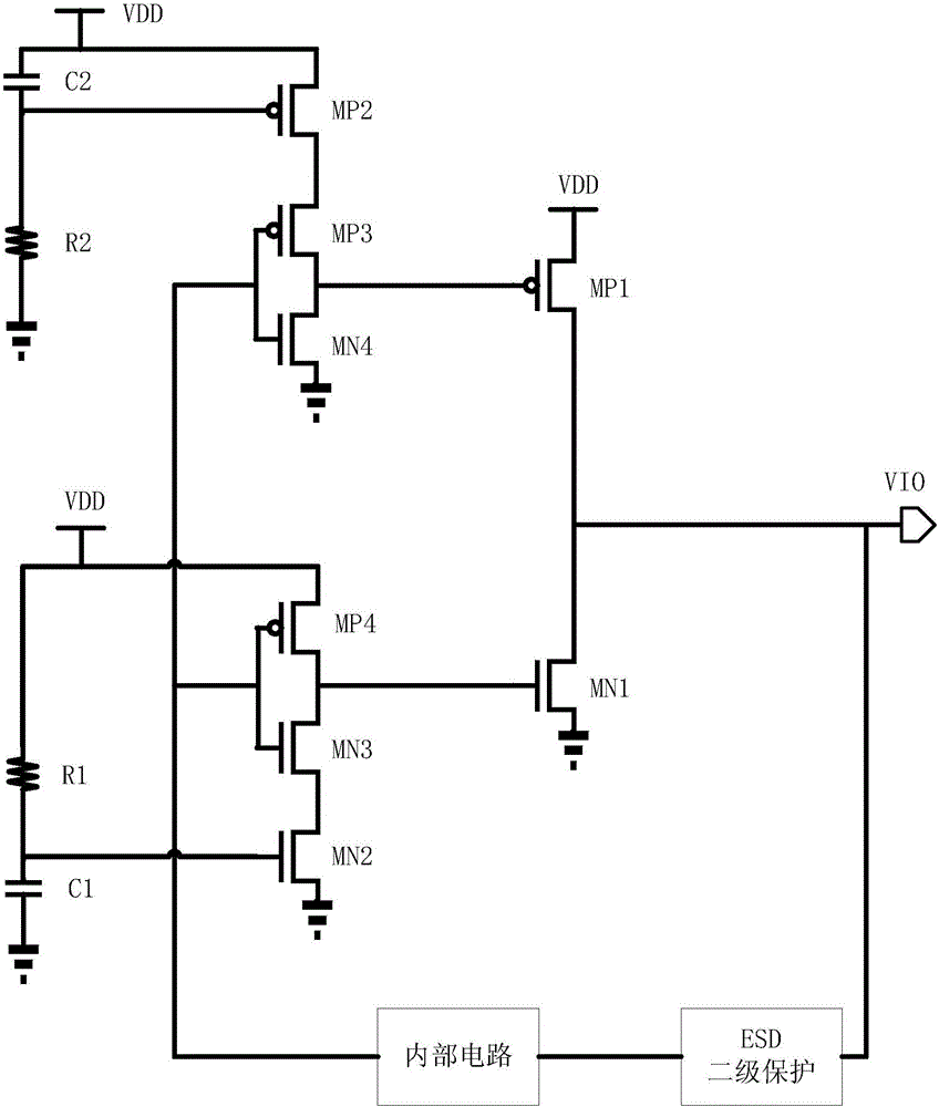
[0018] Please refer to figure 1 As shown, the IO circuit realized by the present invention is as figure 1 As shown, the IO circuit includes: resistor R, capacitor C, pre-stage drive circuit, large-size NMOS, and large-size PMOS. If necessary, an ESD secondary protection circuit can be added, and the ESD secondary protection circuit is set between the internal circuit and the external pin VIO for output.

[0019] The internal circuit in the figure is the internal circuit of the existing IO circuit, and will not be described again.

[0020] Wherein, the resistor R and the capacitor C constitute a ...


PUM


Abstract

The invention discloses an IO circuit used for enhancing ESD performance. The IO circuit comprises a detection circuit, a preceding-stage driving circuit, an ESD protection tube and an IO driving tube. The detection circuit is formed through connecting a resistor and a capacitor in series. The preceding-stage driving circuit is formed by a MOS with a moderate size. The ESD protection tube and the IO driving tube are reused and are formed by a large-size NMOS and a large-size PMOS. The resistor R and the capacitor C form the detection circuit. The detection circuit can detect an ESD event and is served as input of preceding stage driving. The preceding-stage driving circuit controls switches of the large-size NMOS and the large-size PMOS. The large-size NMOS and the large-size PMOS timely and effectively release static electricity in the ESD event and are taken as driving tubes of the IO circuit during normal working. Compared to a conventional method, by using the IO circuit of the invention, in order to reach a same ESD level, needed NMOS and PMOS areas are greatly reduced and a circuit area is effectively decreased through reusing of an ESD protection device and the driving tube.

Description

technical field [0001] The invention belongs to the technical field of chips, in particular to an IO circuit with ESD performance. Background technique [0002] The IO circuit is a bridge connecting the integrated circuit and the external circuit. When ESD (Electro-Static Discharge) occurs, the IO circuit protects itself and the internal circuit. If the IO circuit cannot effectively discharge the static electricity in time, it will cause the integrated circuit to fail. Improve the ESD performance of the IO circuit, so that the integrated circuit needs to have a certain level of ESD to avoid failure in production, transportation, application and other links. [0003] To discharge static electricity, it is necessary to provide a low-resistance path for static electricity. The conventional method is to use the source-drain breakdown of large-size NMOS or PMOS to trigger the parasitic BJT to turn on and enter the snapback, and to release the static electricity in time and effe...

Claims


Application Information

Patent Timeline
Patent Type & Authority Applications(China)
IPC IPC(8): H03K19/0185H01L27/02
Inventor 陆让天
Owner CHIPSEA TECH SHENZHEN CO LTD
Why Eureka
Try Eureka