String contact structure for high voltage ESD

Active Publication Date: 2008-04-24
TAIWAN SEMICON MFG CO LTD
View PDF0 Cites 2 Cited by
  • Summary
  • Abstract
  • Description
  • Claims
  • Application Information

AI Technical Summary

Benefits of technology

[0012]The present invention generally relates to an electrostatic discharge (ESD) protection scheme, and particularly to a string contact structure for an improved ESD performance. Me

Problems solved by technology

When a static charge moves in an integrated circuit (IC), it becomes a current that damages or destroys gate oxide, metallization, and junctions.
Electrostatic charges may accumulate and cause potentially destructive effects on a semiconductor IC device.
ESD damage to a single IC in an electronic device can partially or sometimes completely stop its operation.
As semiconductor processing technology has advanced into deep submicron regimes, the resulting scaled-down semiconductor devices including shallower junction depth and thinner gate oxide layers are less tolerant to ESD stress.
Generally, damage to a device by the ESD event is determined by the device's ability to dissipate the energy of the discharge or withstand the current levels involved.
The models used to perform component testing cannot replicate the full spectrum of all possible ESD events.
Some devices may be more easily damaged by discharges occurring within the automated equipment, while others may be more prone to damage from handling by personnel.
O

Method used


Image

  • String contact structure for high voltage ESD
  • String contact structure for high voltage ESD
  • String contact structure for high voltage ESD

Examples


Example

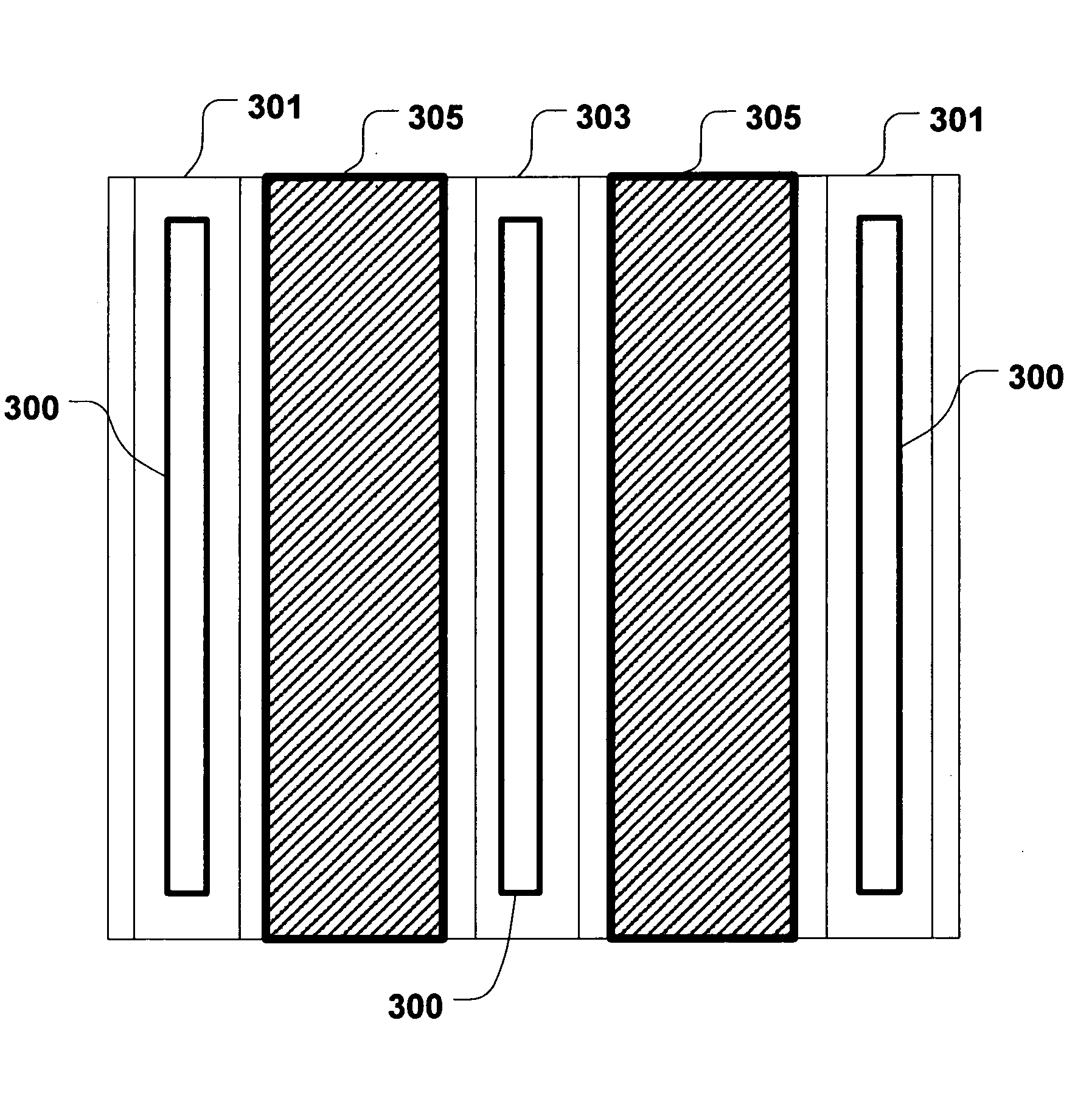
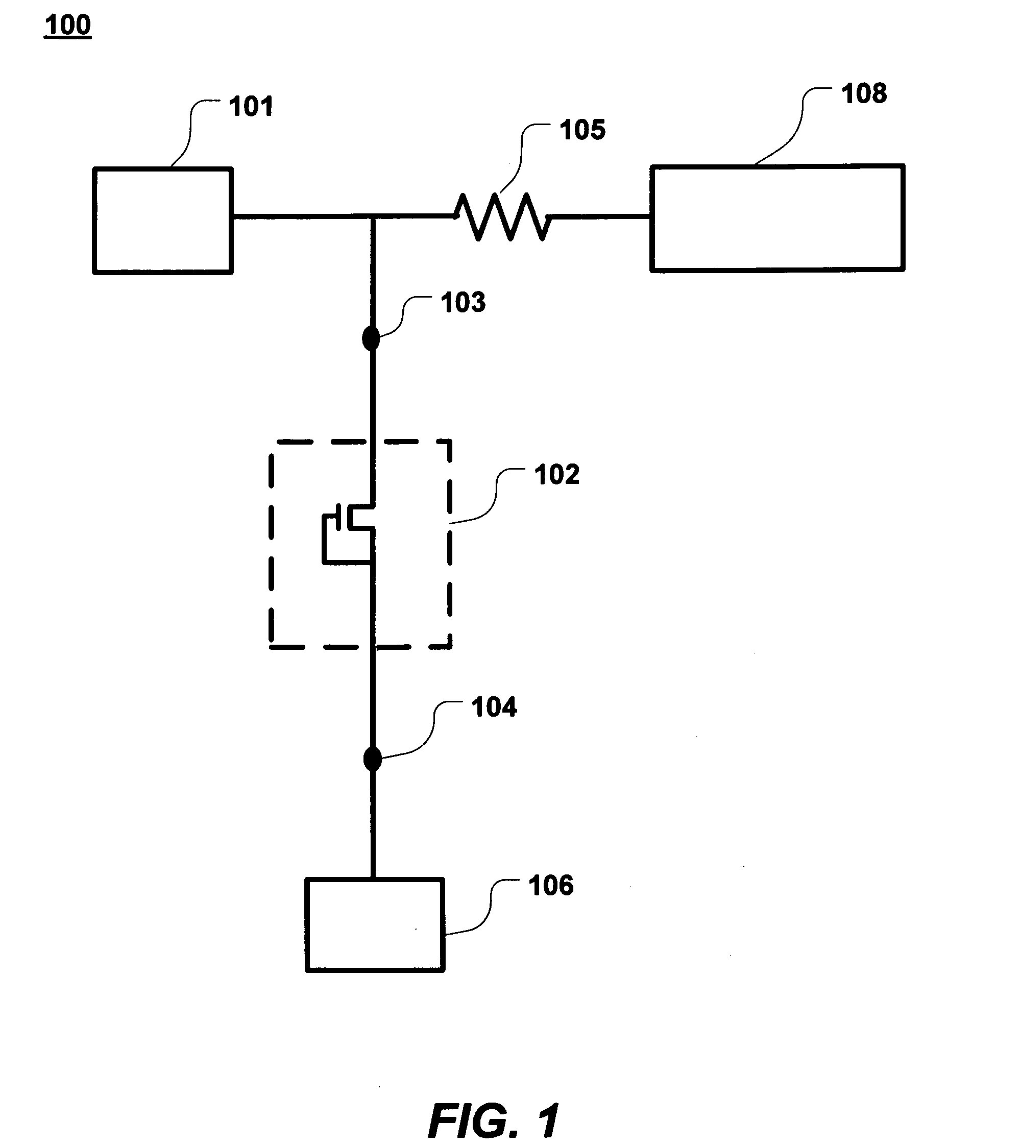
[0024]FIG. 1 is a simplified schematic showing an ESD protection system. The pad 101 may be an input / output (I / O) pad or a power supply (Vdd) pad. A clamp device 102 is connected between the pad 101 and a ground (GND) pad 106 to protect the internal circuit 108 from the ESD voltage appearing on the pad 101. The clamp device 102 is the primary ESD protection device that protects against ESD surges at the I / O pad by clamping the voltage and allowing the high ESD current to be discharged safely to the ground terminal 106.

[0025]An example of the clamp device is a diode chain consisting of one or more diodes connected in series or a grounded-gate NMOS (GGNMOS) transistor having a gate terminal, a source terminal, and a drain terminal. The clamp device including the diode chain, GGNMOS transistor, or the combination thereof is typically coupled in parallel to a protected device or an internal circuit 108, between the I / O pad 101 and a ground pad 106. The clamp device 102 is designed to be...


PUM


Abstract

The present invention relates to an electrostatic discharge (ESD) protection scheme and particularly to a string contact structure for an improved ESD performance. In an embodiment, the invention provides a method for forming an ESD protection circuit for protecting an internal circuit from damage due to an ESD voltage appearing on a pad coupled to a clamp device including a first terminal and a second terminal. The method includes forming a string contact along the first terminal and the second terminal of the clamp device. The method further includes forming one or more conductive layers on the string contact to couple the first terminal and the second terminal of the clamp device to the pad and a ground pad.

Description

BACKGROUND OF THE INVENTION[0001]The present invention generally relates to an electrostatic discharge (ESD) protection scheme, and particularly to a string contact structure for an improved ESD performance.[0002]Electrostatic discharge (ESD) is the sudden and momentary electric current that flows when an excess of electric charge, stored on an electrically insulated object, finds a path to an object at a different electrical potential such as ground. When a static charge moves in an integrated circuit (IC), it becomes a current that damages or destroys gate oxide, metallization, and junctions. ESD can occur when a charged body touches an IC, a charged IC touches a grounded surface, or a charged machine touches an IC.[0003]ESD is a common phenomenon that occurs during the handling of semiconductor devices. Electrostatic charges may accumulate and cause potentially destructive effects on a semiconductor IC device. ESD stress can occur during a testing phase of IC fabrication, during ...

Claims


Application Information

Patent Timeline
IPC IPC(8): H01L23/62
CPCH01L23/60H01L27/0288H01L2924/0002H01L2924/00
Inventor PERNG, D. J.CHEN, SHUI-HUNGLEE, JIAN-HSINGYUNG-SHENG, HUANG
Owner TAIWAN SEMICON MFG CO LTD
Why Eureka
Try Eureka