

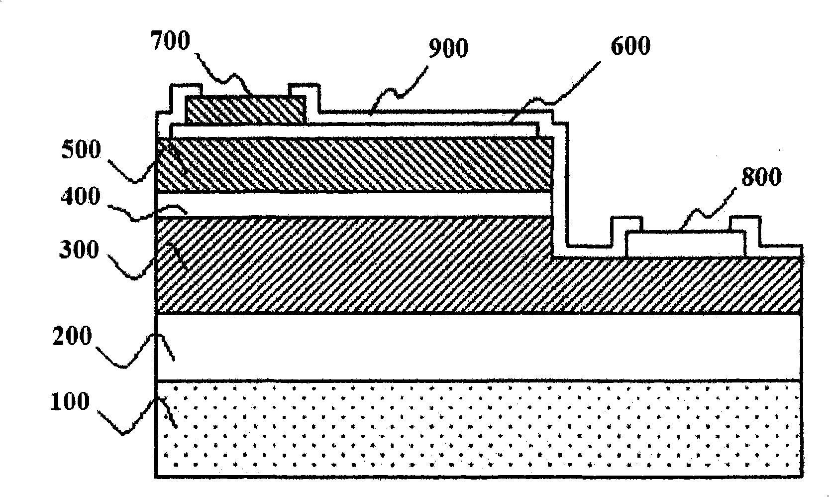
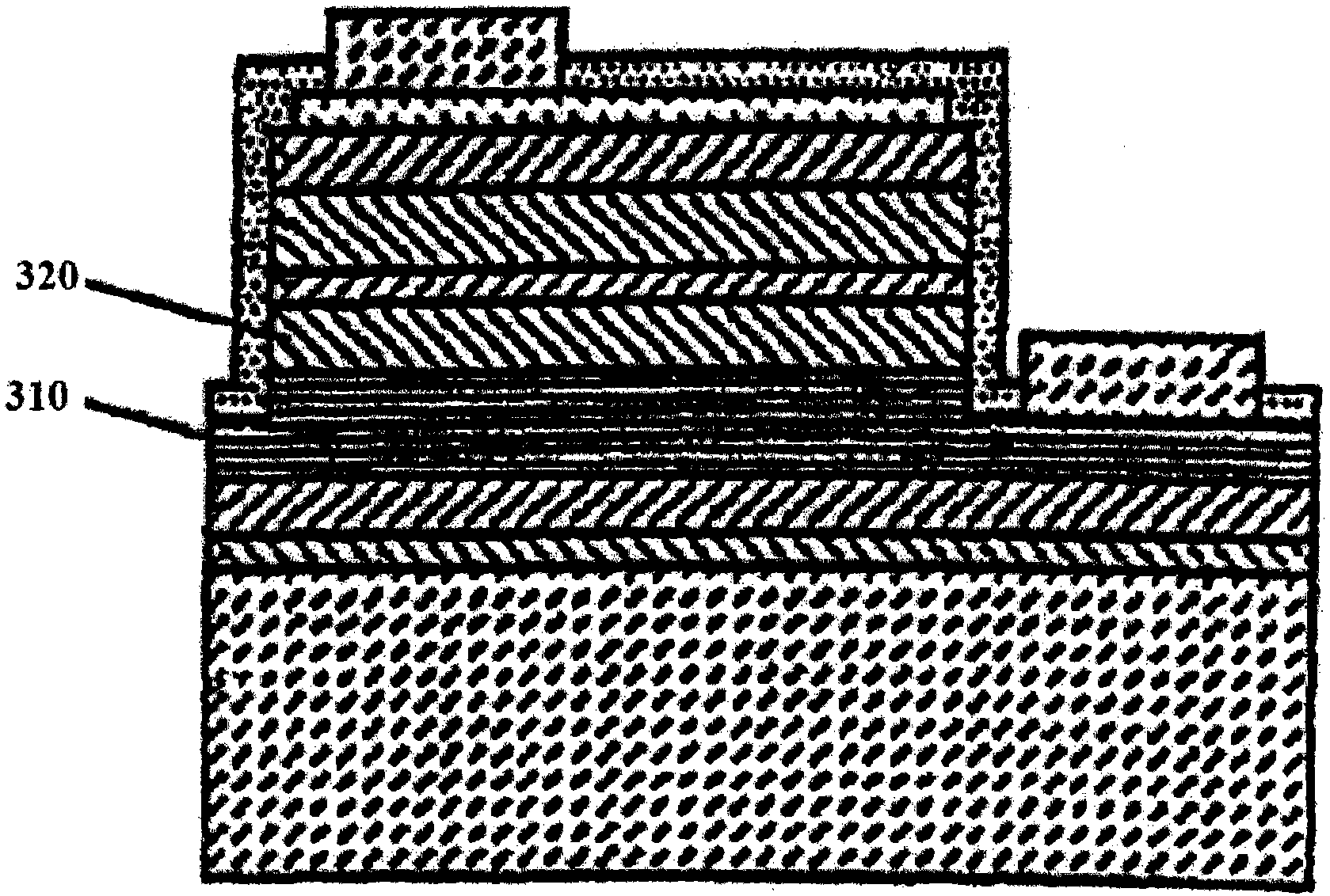
III-nitride semiconductor light emitting device
A technology of nitride semiconductors and light-emitting devices, which is applied in the direction of semiconductor devices, electrical components, circuits, etc., can solve problems such as difficult manufacturing, and achieve the effect of promoting current expansion and improving ESD characteristics
- Summary
- Abstract
- Description
- Claims
- Application Information
AI Technical Summary
Problems solved by technology
Method used
Image

Examples
Embodiment Construction
[0051] Hereinafter, the present invention will be described in detail with reference to the accompanying drawings.
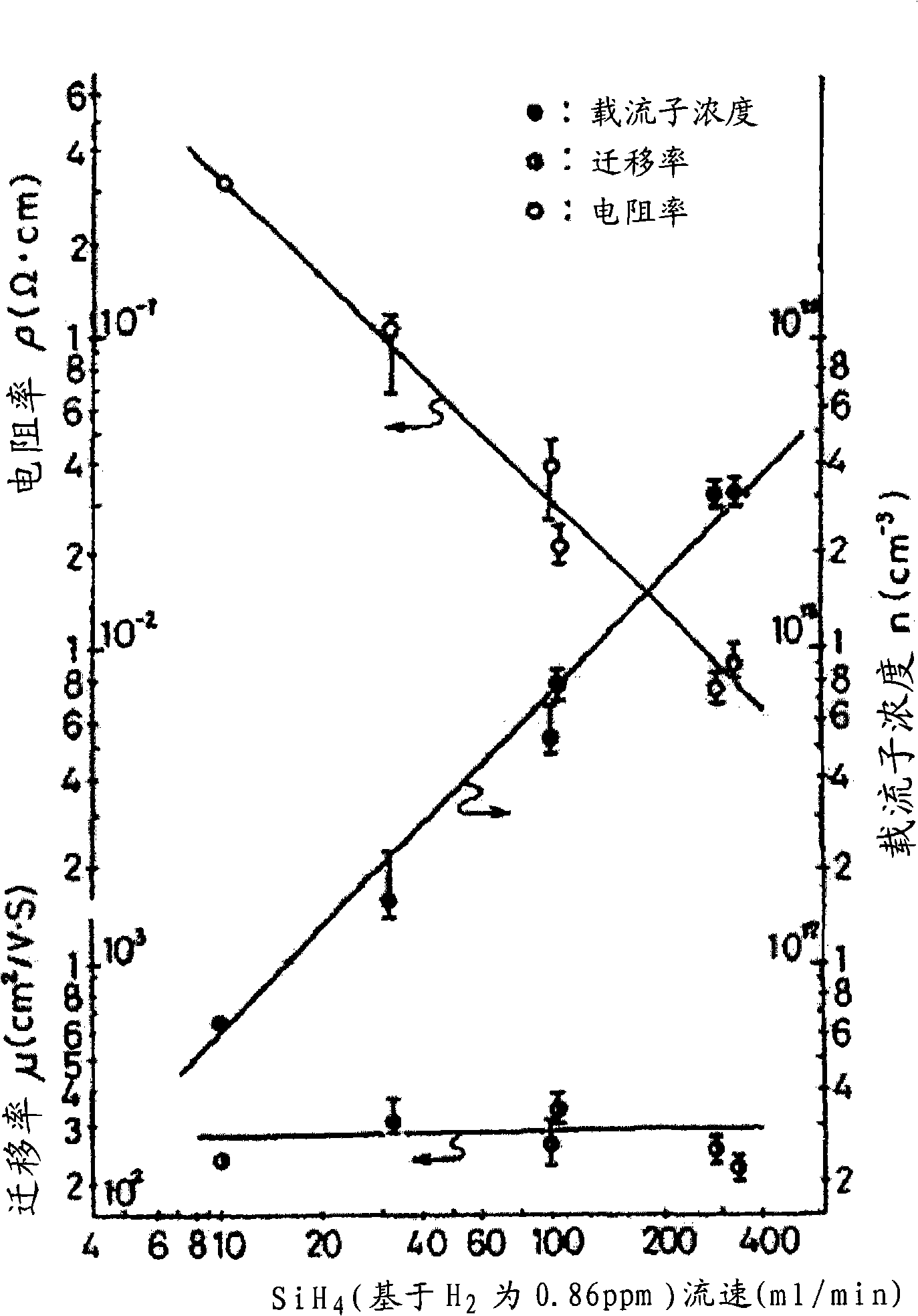
[0052] Figure 6 is a view describing an experimental example of the present invention, specifically, a surface micrograph (left side) showing a state in which 5×10 19 / cm 3 doping concentration (9.5sccm of DTBSi supplied as Si source) and thickness of the n-type GaN layer and having The thickness of the un-GaN layer (by adjusting the supply time of the Si source, for example, supplying the Si source for 15 seconds and stopping the supply for 25 seconds) to grow an n-type nitride semiconductor layer having a thickness of about 2 μm, and a surface showing the following state Microscopic photographs (right side): in which an n-type nitride semiconductor layer was grown under different conditions by supplying 9.0 sccm of DTBSi as a Si source. This experiment is used to study whether it can pass from such as 5×10 19 / cm 3 The high-concentration doping reduce...
PUM
 Abstract
Description
Claims
Application Information