
Selective deposition of germanium spacers on nitride

a germanium spacer and selective deposition technology, applied in the direction of semiconductor devices, electrical apparatus, transistors, etc., can solve the problems of increasing the dose of implanted dopants, reducing the thickness of gate dielectrics below 2 nm, and high leakage devices in short channels fet, so as to reduce the depletion of polysilicon in the gate. , the effect of increasing the dose of implantation

Inactive Publication Date: 2007-03-15
GLOBALFOUNDRIES INC
View PDF18 Cites 4 Cited by
  • Summary
  • Abstract
  • Description
  • Claims
  • Application Information

AI Technical Summary

Benefits of technology

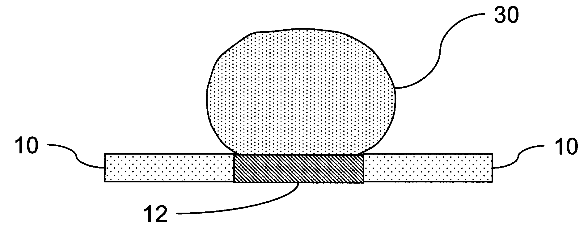
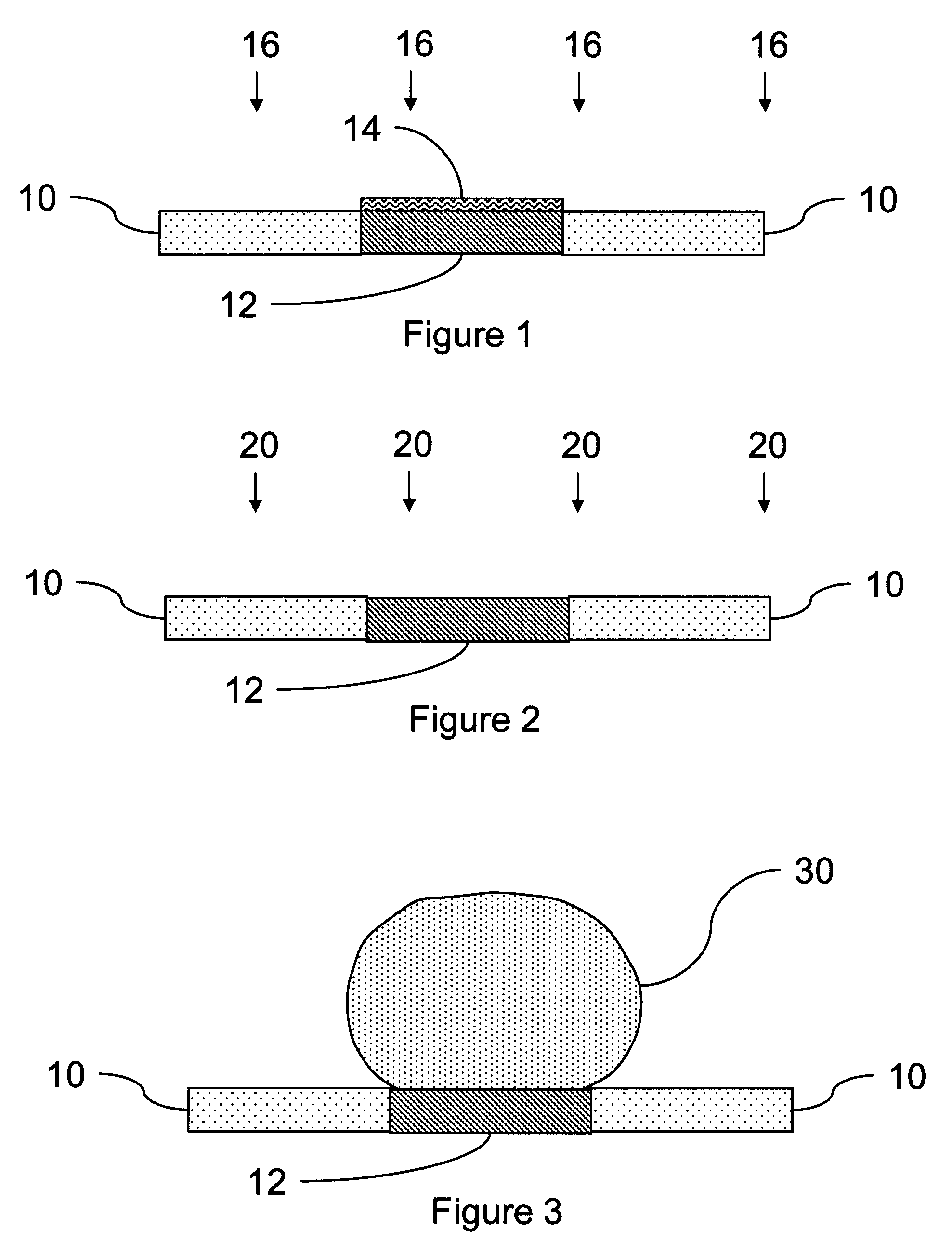
[0005] The COR process of treating the nitride surface comprises exposing the wafer surface to a mixture of gaseous HF and NH3. For example, the HF and NH3 flow can be supplied in a flow ratio of 1:10 to 10:1. The gas is supplied at a pressure between 1 to 15 mTorr for between about 5 seconds and about 300 seconds. This COR process removes any native oxide or oxynitride from the nitride surface and leaves the nitride surface in such as state that it can nucleate the subsequent germanium deposition. One feature is that this COR process is a vapor phase process substantially free of water. Water in a liquid or vapor phase can easily reoxidize the nitride surface so minimizing water in this process is advantageous.
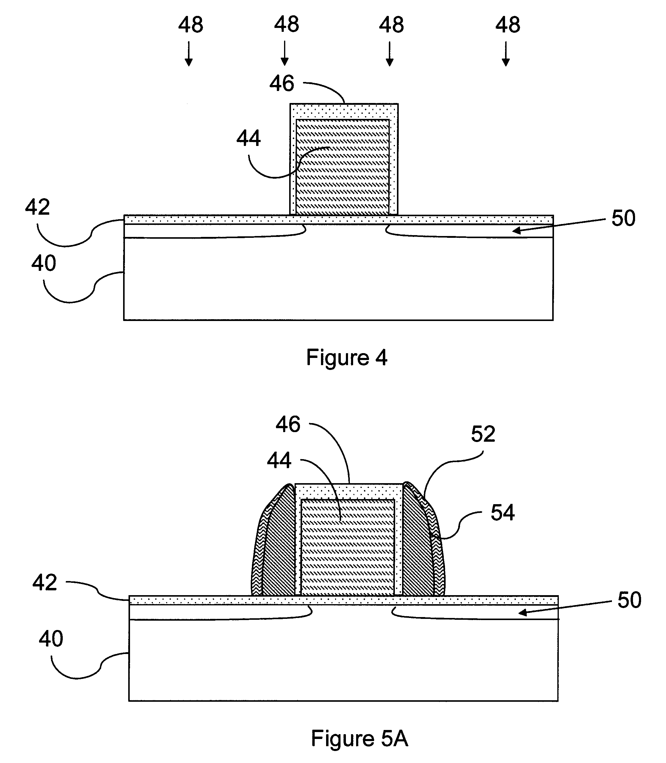
[0008] The inventive methodology can be utilized to manufacture many different types of structures. For example, the invention can be utilized to create temporary spacers during the formation of field effect transistors. In this method, the invention implants source / drain extension implants into a substrate having patterned gate conductor structures. Next, the invention forms nitride spacers adjacent the gate conductor structures. The native oxide is removed from the nitride surface and then the nitride spacers are exposed to a heated germanium containing gas such as germane (GeH4) to selectively form germanium structures only on the nitride spacers. After this, using the germanium structures as large masking sidewalls, the invention implants source and drain implants into the gate and substrate. Because the wide germanium spacer structure offsets the source and drain implant away from the critical gate and channel region, the implantation dose can be increased to reduce polysilicon depletion in the gate. Then, the germanium structures can be removed and remaining elements of the field effect transistor can be completed.

Problems solved by technology

However, it becomes increasingly more difficult to reduce the gate dielectric thickness below 2 nm because of exponentially increasing gate leakage current from direct tunneling through the thin gate dielectric layer.
However, in a conventional FET fabrication process, simply increasing the dose of the implanted dopants is problematic because the source / drain is doped at the same time as the gate.
When the doping in the source drain region becomes too high, the source and drain diffuse towards each other underneath the gate electrode, creating a high leakage device in short channel FET.

Method used


Image

  • Selective deposition of germanium spacers on nitride
  • Selective deposition of germanium spacers on nitride
  • Selective deposition of germanium spacers on nitride

Examples


Embodiment Construction

[0022] The present invention and the various features and advantageous details thereof are explained more fully with reference to the nonlimiting embodiments that are illustrated in the accompanying drawings and detailed in the following description. It should be noted that the features illustrated in the drawings are not necessarily drawn to scale. Descriptions of well-known components and processing techniques are omitted so as to not unnecessarily obscure the present invention. The examples used herein are intended merely to facilitate an understanding of ways in which the invention may be practiced and to further enable those of skill in the art to practice the invention. Accordingly, the examples should not be construed as limiting the scope of the invention. Semiconductor processing techniques are well known in the art and can be found in many references. By way of example, reference may be had to Silicon Processing For the VLSI Era, Lattice Press 1990; U.S. Pat. No. 5,573,965...


PUM

PropertyMeasurementUnit
temperatureaaaaaaaaaa
thicknessaaaaaaaaaa

Abstract

A method of selectively forming a germanium structure within semiconductor manufacturing processes removes the native oxide from a nitride surface in a chemical oxide removal (COR) process and then exposes the heated nitride and oxide surface to a heated germanium containing gas to selectively form germanium only on the nitride surface but not the oxide surface.

Description

FIELD OF THE INVENTION [0001] The invention generally relates to a method of selectively forming a semiconductor (germanium) structure within semiconductor manufacturing processes that treats a nitride and oxide surface with a chemical oxide removal (COR) process and then heats and exposes the nitride, semiconductor and oxide surface, to a heated semiconductor (germanium) containing gas to selectively form semiconductor (germanium) only on the nitride and semiconductor surface, but not on the oxide surface. DESCRIPTION OF THE RELATED ART [0002] Standard semiconductor manufacturing processes use combinations of deposited, grown and patterned oxide, nitride and semiconductor along with doping and thermal treatments to form transistors which are subsequently interconnected to form integrated circuits. Selectively deposited or grown structures which utilize combinations of oxide, nitride and semiconductors are of great use in semiconductor manufacturing because selectivity enables const...

Claims


Application Information

Patent Timeline
Patent Type & Authority Applications(United States)
IPC IPC(8): H01L21/336H01L21/44H01L21/20
CPCH01L21/02532H01L21/02587H01L21/0262H01L21/02639H01L29/665H01L29/6653H01L29/6656H01L2924/1305H01L29/6659H01L29/7833H01L2224/10126H01L2224/13023H01L2924/00H01L2224/05571H01L2224/05573
Inventor CHAKRAVARTI, ASHIMA B.CHOU, ANTHONY I.FURUKAWA, TOSHIHARUHOLMES, STEVEN J.NATZLE, WESLEY C.
Owner GLOBALFOUNDRIES INC
Learn More