Supporting plate, apparatus, and method for stripping supporting plate

Inactive Publication Date: 2007-03-22
TOKYO OHKA KOGYO CO LTD
View PDF7 Cites 90 Cited by
  • Summary
  • Abstract
  • Description
  • Claims
  • Application Information

AI Technical Summary

Benefits of technology

[0032] Since the stripping method of the present invention comprises the steps of supplying a solvent from outside to a second penetrating hole of a plate, distributing the solvent from a second penetrating hole of a supporting plate to grooves connecting with the second penetrating hole of the supporting plate, dissolving the adhesive on a surface contacted with the sub

Problems solved by technology

In the above-mentioned techniques, since it is difficult for a solvent to enter between the supporting plate (protecting tape) and the semiconductor wafer when the supporting plate (protecting tape) is stripped from the semiconductor wafer, it takes too much time to strip the supporting plate from the semiconductor wafer.
Also, the thermoplastic film bonding the support plate (protecting tape) and the semiconductor wafer often fails to completely dissolve, and tends to be left in a state of sticking to either the support plate or the semiconductor wafer.
If an adhesive is left as described above, cracking or chipping of the semiconductor wafer easily occurs at the

Method used


Image

  • Supporting plate, apparatus, and method for stripping supporting plate
  • Supporting plate, apparatus, and method for stripping supporting plate
  • Supporting plate, apparatus, and method for stripping supporting plate

Examples


Embodiment Construction

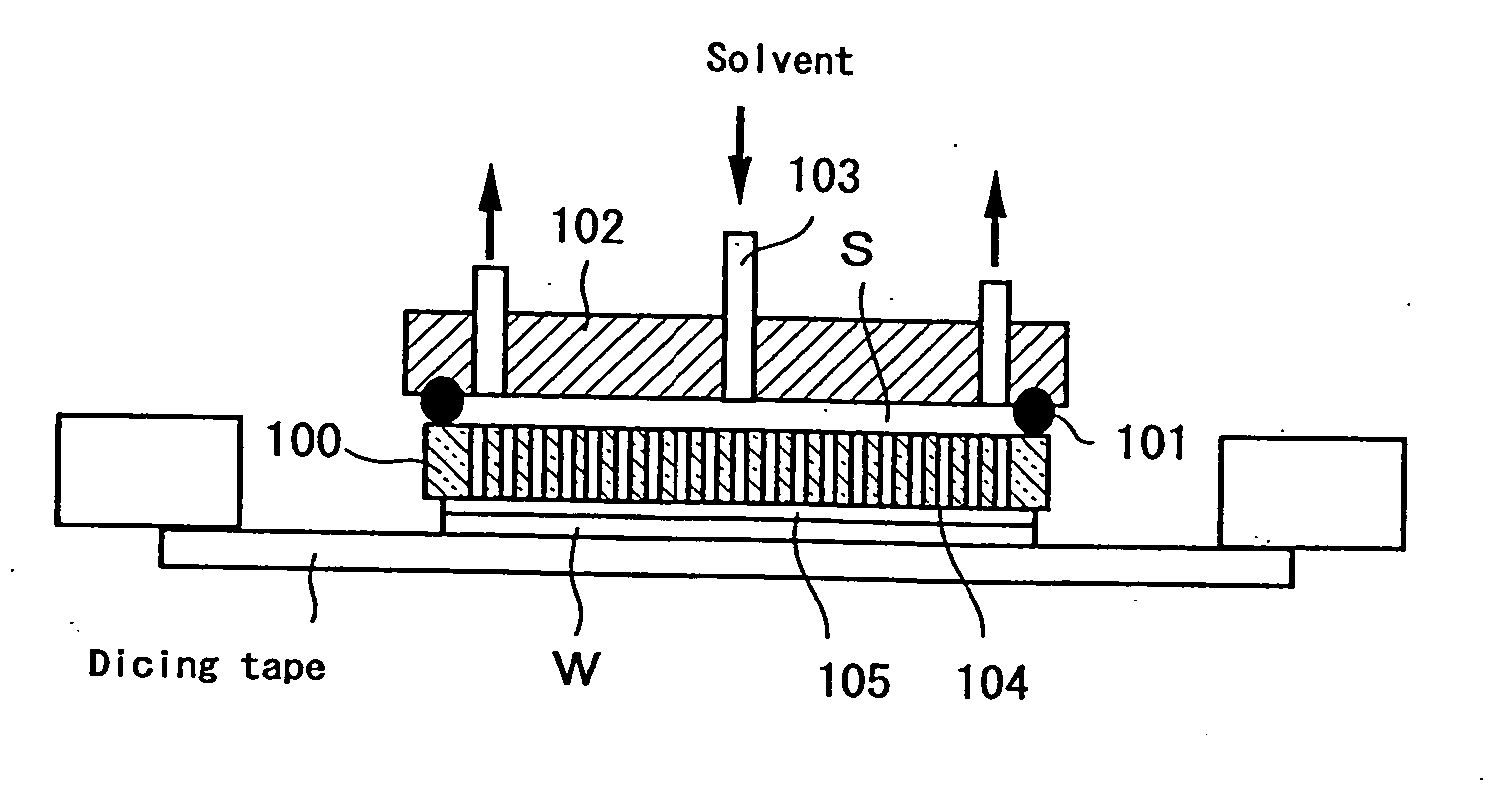
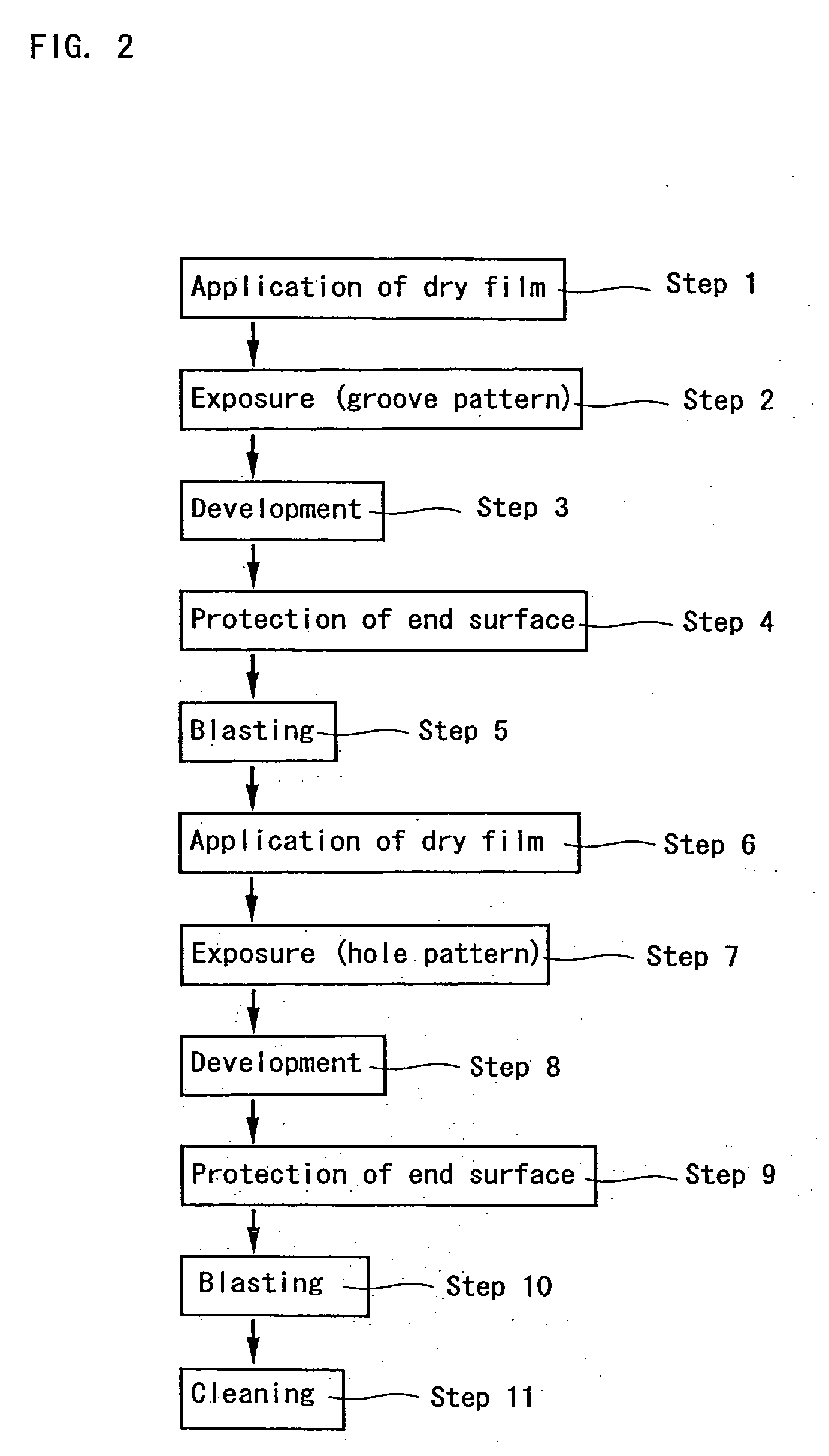
[0043] Embodiments of the present invention will be described below with reference to the attached drawings. FIG. 1 is a schematic view showing an embodiment of a supporting plate according to the present invention, and FIG. 2 shows the process for forming a supporting plate.

[0044] A supporting plate 1 according to the present invention shown in FIG. 1 is made of a glass plate, a ceramic plate or a metal plate.

[0045] A circuit-formed surface of a semiconductor wafer W is bonded to one of the surfaces of the supporting plate 1 by using an adhesive, which is not shown in the drawing.

[0046] According to the present invention, the supporting plate 1 has a unique structure as described below.

[0047] A first penetrating hole 2 is formed in a substantially central portion (center) of the supporting plate 1 so as to penetrate in the thickness direction. A plurality of first penetrating holes 2 may be formed, and for example, four penetrating holes 2 are formed in FIG. 1. However, the num...


PUM

PropertyMeasurementUnit
Timeaaaaaaaaaa
Thicknessaaaaaaaaaa

Abstract

A supporting plate which makes it possible to easily strip the supporting plate from a substrate in a short period of time after thinning the substrate. In the supporting plate to which a circuit-formed surface of a substrate is bonded with an adhesive, a first penetrating hole is formed in a substantially central portion of the supporting plate in the thickness direction, grooves connecting with the first penetrating hole are formed on a surface of the supporting plate to be contacted with an adhesive, and a second penetrating hole connecting with the grooves is formed in a peripheral portion of the supporting plate in the thickness direction.

Description

BACKGROUND OF THE INVENTION [0001] 1. Field of the Invention [0002] The present invention relates to a supporting plate which is used when a substrate such as a semiconductor wafer is thinned, and also relates to an apparatus and a method for stripping the supporting plate from the semiconductor wafer. [0003] 2. Description of the Prior Art [0004] There is a continuing need to make IC cards and cell phones thinner, smaller, and lighter. In order to satisfy this need, semiconductor chips to be incorporated therein must be thin. Although at present the thickness of a wafer which forms a semiconductor chip is 125-150 μm, it is expected that the thickness of a semiconductor wafer must be 25-50 μm for a next generation of chips. [0005] An example of a conventional method for thinning a semiconductor wafer is shown in FIG. 8. Specifically, a protecting tape is attached to a surface (A-surface) of a semiconductor wafer on which a circuit (element) has been formed. The wafer is turned over,...

Claims


Application Information

Patent Timeline
IPC IPC(8): B29C63/00
CPCB29C63/0013B29L2031/3425Y10T156/1132Y10T156/1928Y10T156/1111H01L21/304H01L21/683H01L21/687
Inventor NAKAMURA, AKIHIKOMIYANARI, ATSUSHIINAO, YOSHIHIRO
Owner TOKYO OHKA KOGYO CO LTD
Why Eureka
Try Eureka