OLED device having improved light output

a light-emitting diode and light-emitting layer technology, which is applied in the direction of organic semiconductor devices, discharge tubes/lamp details, discharge tubes luminescnet screens, etc., can solve the problems of limiting affecting the light output of oled light-emitting layers, and affecting the efficiency of oled devices, so as to achieve the effect of increasing the light output and maintaining the sharpness of oled devices

Active Publication Date: 2007-03-22
GLOBAL OLED TECH
View PDF14 Cites 45 Cited by
  • Summary
  • Abstract
  • Description
  • Claims
  • Application Information

AI Technical Summary

Benefits of technology

The present invention improves the brightness of OLED devices without compromising their clarity.

Problems solved by technology

The patent text describes a problem in improving the out-coupling of light from organic light-emitting diodes (OLEDs) by using scattering layers and reflective electrodes. However, these techniques suffer from absorption and trapping of light in the OLED device and incomplete light extraction. The patent text proposes an improved structure that avoids these issues and improves the efficiency and sharpness of the device.

Method used


Image

  • OLED device having improved light output
  • OLED device having improved light output
  • OLED device having improved light output

Examples


Embodiment Construction

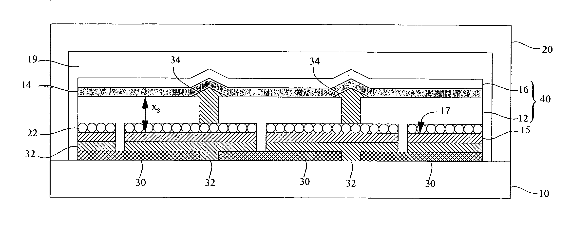
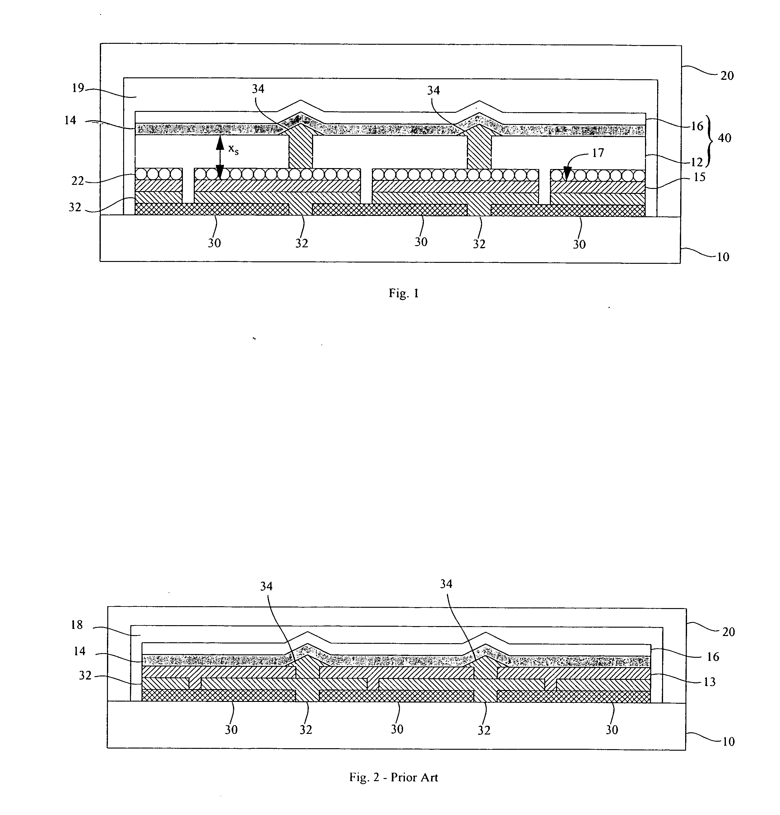
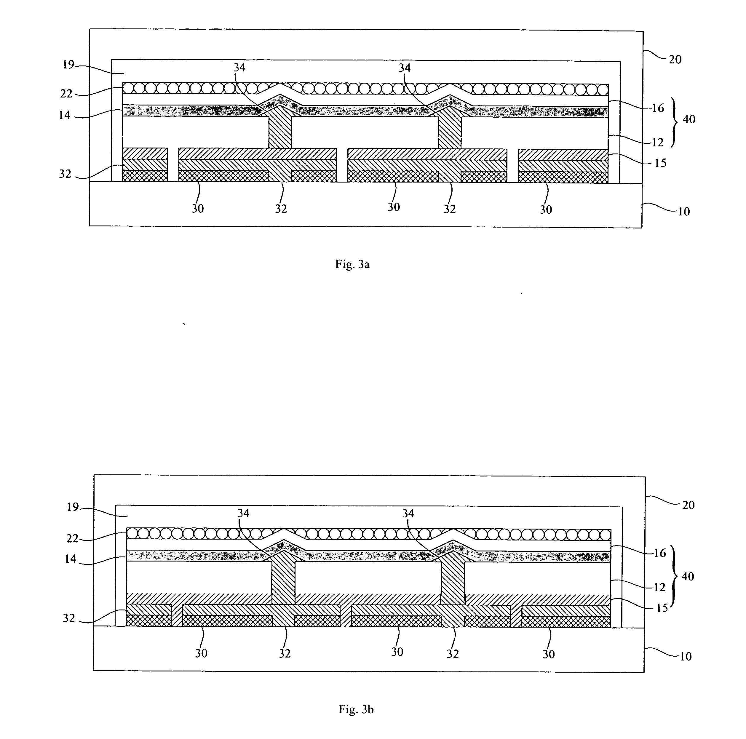
[0031] As described above, light generated within an OLED device can be emitted from the device, confined in the substrate or cover, or confined in the organic layers and electrodes. Materials having free electrons in the conduction band, for example metals, support formation of surface plasmons-polaritons in the presence of a radiating dipole. In the visible portion of the electromagnetic spectrum, such materials typically also have a dielectric constant with a negative real part. Accordingly, if a metallic, light-reflective electrode layer surface is located in proximity to an OLED emissive layer, some electrical energy may be converted to optical energy by the dipole that may then excite surface plasmons-polaritons (SP) at the metallic layer surface. Although it is true that SP modes are waveguide modes, the nature of SP waveguide modes differs significantly from that of Modes I, II, or III emitted light. First of all, the electromagnetic fields of SP modes are confined very clos...


PUM


Abstract

An organic light-emitting diode (OLED) device, comprising: first and second transparent electrodes, and one or more layers of organic material formed between the first and second transparent electrodes, the layers of organic material including one or more light-emitting layers; a reflective layer having a surface plasmon-polariton supporting reflective surface located on a side of either of the first or second transparent electrodes opposite to the organic material layers; and a scattering layer in optical contact with the organic material layers and the electrodes. In certain embodiments, layer spacing is preferably designed such that the distance between the reflective surface and at least one of the one or more light-emitting layers is equal to or greater than 60 nm. Additionally, a low-index layer is preferably employed in various embodiments to improve device sharpness.

Description


Claims


Application Information

Patent Timeline
Owner GLOBAL OLED TECH
Why Eureka
Try Eureka