Jig for manufacturing semiconductor devices and method for manufacturing the jig

Inactive Publication Date: 2007-03-29
LAPIS SEMICON CO LTD
View PDF62 Cites 16 Cited by
  • Summary
  • Abstract
  • Description
  • Claims
  • Application Information

AI Technical Summary

Benefits of technology

[0011] An object of the present invention is to provide a jig for use with a semiconductor m

Problems solved by technology

The aforementioned conventional method for dicing a semiconductor wafer suffers from the following problems.
If bumps and wires are formed on the back surface of a semiconductor wafer for electrically connecting the chips to a wiring substrate, the bumps and wires may interfere with the dicing jig to create air gaps between the semiconductor wafer and the dicing tape.
Especially, when the partition regions of the semiconductor wafer are not in intimate contact with the dicing tape, if the semiconductor wafer is moved relative to the dicing tape or is s

Method used


Image

  • Jig for manufacturing semiconductor devices and method for manufacturing the jig
  • Jig for manufacturing semiconductor devices and method for manufacturing the jig
  • Jig for manufacturing semiconductor devices and method for manufacturing the jig

Examples


first embodiment

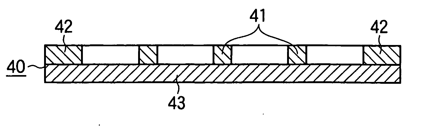
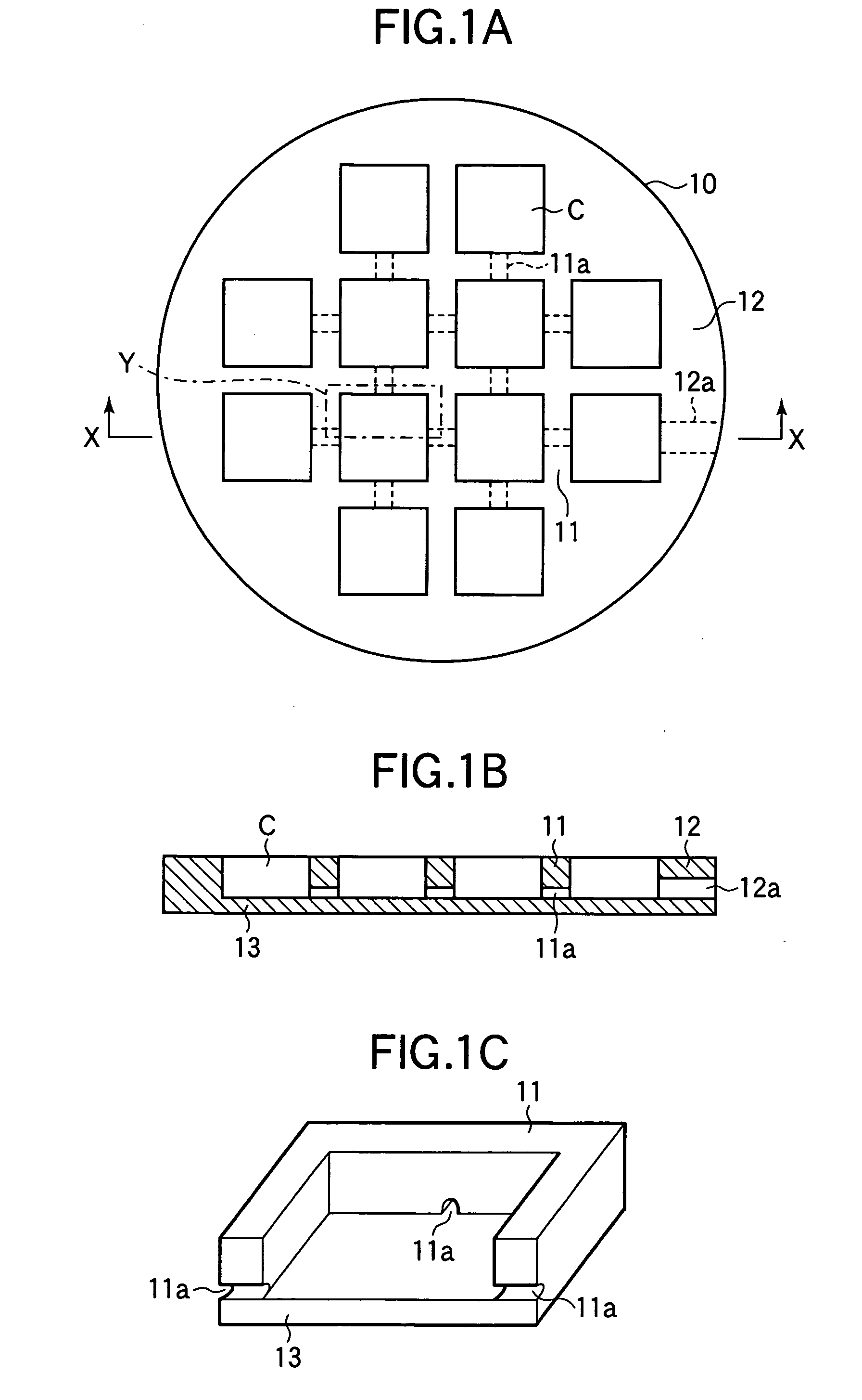
[0049]FIG. 1A is a top view illustrating a dicing jig 10 of the first embodiment. FIG. 1B is a cross sectional view taken along a line X-X of FIG. 1A. FIG. 1C is an enlarged view of a portion depicted at Y in FIG. 1A.

[0050] Referring to FIGS. 1A and 1B, the dicing jig 10 is of a one piece construction that includes partitions 11, an outer frame 12 formed to surround the partitions 11, a bottom 13 on which the partitions and the outer frame 12 are formed. The outer frame 12 has an outer diameter larger than that of a semiconductor wafer W (FIG. 2A).

[0051] The partitions 11 and outer frame 12 have the same height so that their top surfaces extend in the same plane. The partitions 11 define individual cavities C that are in communication with adjacent cavities via communication holes 11a formed in the partitions 11. An inlet / outlet 12a is formed in the outer frame 12 through which air in the individual cavities are evacuated or air is let in the cavities.

[0052] The dicing jig 10 is ...

second embodiment

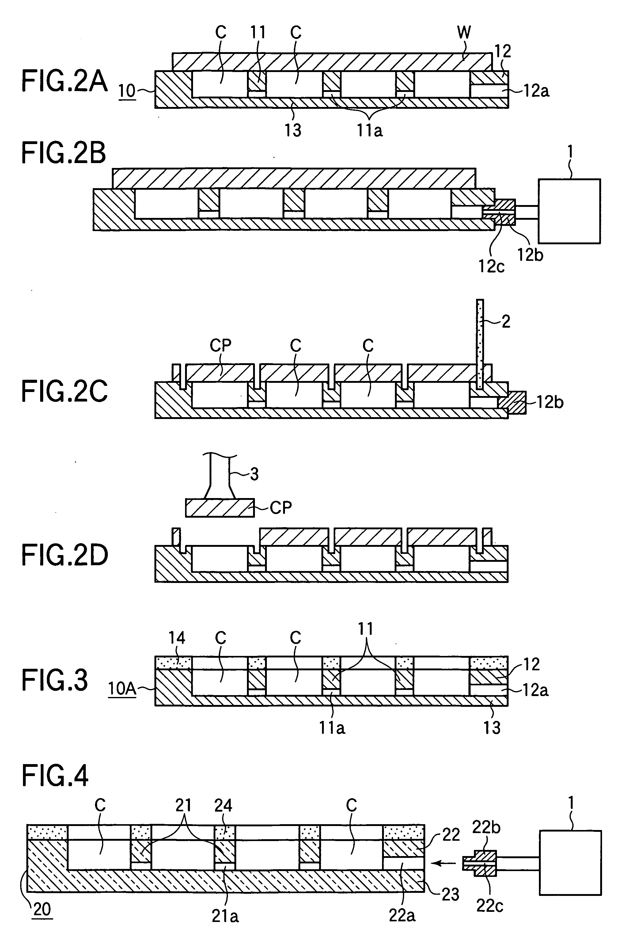
[0058]FIG. 3 is a cross sectional view corresponding to FIG. 1B, illustrating the configuration of a dicing jig 10A of a second embodiment.

[0059] The dicing jig 10A differs from the dicing jig 10 in that a layer 14 is formed of a resilient resin material such as poly-silicone or silicone rubber and is placed on the top surfaces of partitions 11 and outer frame 12. The layer 14 has a thickness of about 0.1 mm. The layer 14 may be formed by applying a resin material to the surfaces or by attaching a pre-shaped thin resin film onto the top surfaces.

[0060] The dicing jig 10A can be used to dice a semiconductor wafer W in much the same way as the first embodiment. The semiconductor wafer W is placed on the dicing jig 10A such that the dicing regions of the semiconductor wafer W sit on the layer 14. A plug 12b having a needle 12c inserted therein is attached into an inlet / outlet 12a. Then, a vacuum pump 1 is connected to the inlet / outlet 12a to evacuate the air from the cavities C throu...

third embodiment

[0064]FIG. 4 is a cross-sectional view corresponding to FIG. 1B, illustrating the configuration of a dicing jig 20 of a third embodiment.

[0065] The dicing jig 20 includes partitions 21, an outer frame 22, a bottom 23, and a layer 24 of UV curing resin formed on the top surfaces of the partitions 21 and the outer frame 22. Cavities C are defined between the partitions 21 and between the partitions 21 and the outer frame 22. The cavities C communicate with one another through communication holes 21a.

[0066] The dicing jig 20 differs from the dicing jig 10 in FIG. 1 in material. Thatis, the partitions 21, outer frame 22, and bottom 23 are in one piece construction of a UV transmitting material such as glass or plastics. The partitions 21, outer frame 22, and bottom 23 have substantially the same shapes as those in FIG. 1 except that the thickness of bottom 23 needs to be selected according to the mechanical strength of the material of the dicing jig 20.

[0067] The outer frame 12 has a...


PUM

PropertyMeasurementUnit
Pressureaaaaaaaaaa
Transparencyaaaaaaaaaa
Lightaaaaaaaaaa

Abstract

A jig is used for dicing a semiconductor device on which a plurality of chip regions are formed. The jig includes partitions that forms grids and a bottom wall the partitions are supported. When the semiconductor wafer is placed on the jig, the partitions support dicing regions of the semiconductor wafer such that at least one cavity is defined by the semiconductor wafer, the partitions, and the bottom wall. A negative pressure is created in the recesses by evacuating the air from the recesses. The semiconductor wafer is diced at the dicing regions into a plurality chips. The pressure in the recesses is returned to atmospheric pressure. Then, each of the chips is picked up from the jig.

Description

BACKGROUND OF THE INVENTION [0001] 1. Field of the Invention [0002] The present invention relates to a jig for use in dicing a semiconductor wafer and a method for dicing a semiconductor wafer by the use of the jig. [0003] 2. Description of the Related Art [0004] Conventionally, semiconductor wafers in which integrated circuits are fabricated into individual chips were diced in the following conventional process. [0005] A dicing tape is a tape of resin having a predetermined thickness. An adhesive is applied to a surface of the dicing tape. The dicing tape is attached to the entire back surface of a semiconductor wafer. [0006] The semiconductor wafer to which the dicing tape has been attached is placed face up on a dicing apparatus. Then, the semiconductor wafer is attracted to a chuck of the dicing apparatus by vacuum adsorption. [0007] Then, a rotating blade is used to cut the semiconductor wafer along predetermined partition regions that surround individual chip areas. The blade ...

Claims


Application Information

Patent Timeline
IPC IPC(8): C23C16/00
CPCH01L21/6838H01L21/67092
Inventor SAEKI, YOSHIHIRO
Owner LAPIS SEMICON CO LTD
Why Eureka
Try Eureka