Packaged electronic devices and process of manufacturing same

a technology of electronic devices and packaging, applied in the direction of printed circuits, semiconductor devices, semiconductor/solid-state device details, etc., can solve the problems of reducing the efficiency of electronic devices, requiring a significant amount of horizontal space for different electronic devices in a device module, and a relatively high amount of assembly and processing complexity and cost. achieve the effect of reducing radio frequency interferen

Inactive Publication Date: 2007-03-29
SKYWORKS SOLUTIONS INC
View PDF26 Cites 17 Cited by
  • Summary
  • Abstract
  • Description
  • Claims
  • Application Information

AI Technical Summary

Benefits of technology

[0002] An electronic module and process for forming the same are provided. In accordance with exemplary embodiments of the present invention, a second electronic device is arranged above a first electronic device. Spacers are arranged between a first and second electronic device to form a uniform and sealed air gap between the electronic devices. The height of the spacers, and the resulting height of the air gap, is selected based upon the type of electronic device. For radio frequency electronic devices, the height of the spacers is selected to reduce radio frequency interference between the first and second electronic devices. In the case of microelectronic machines, the height is selected to allow sufficient clearance for operation of the machines.

Problems solved by technology

The integration of different electronic devices into a device module typically requires a significant amount of horizontal space, and relatively high assembly and processing complexity and cost.

Method used


Image

  • Packaged electronic devices and process of manufacturing same
  • Packaged electronic devices and process of manufacturing same
  • Packaged electronic devices and process of manufacturing same

Examples


Embodiment Construction

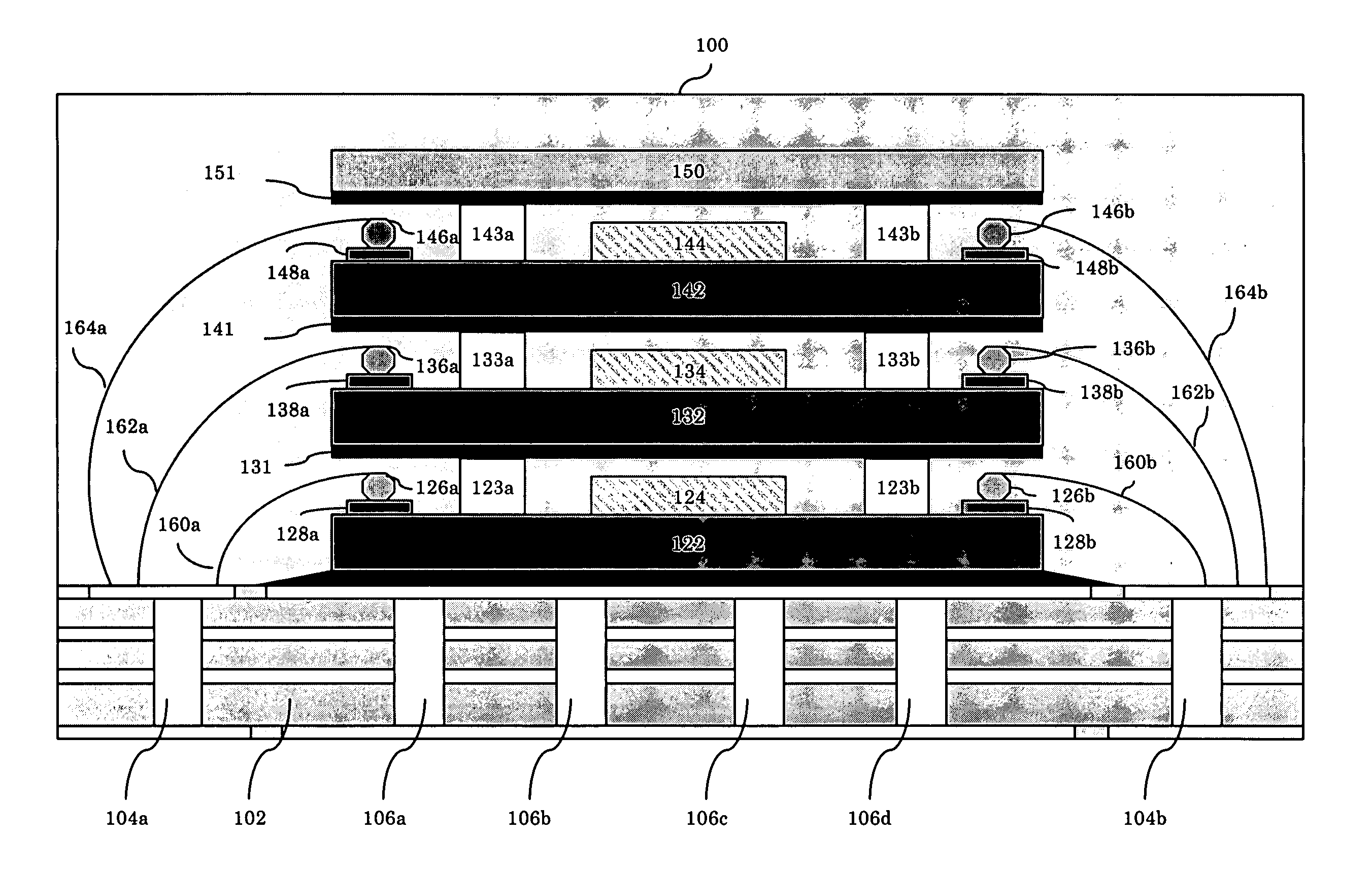
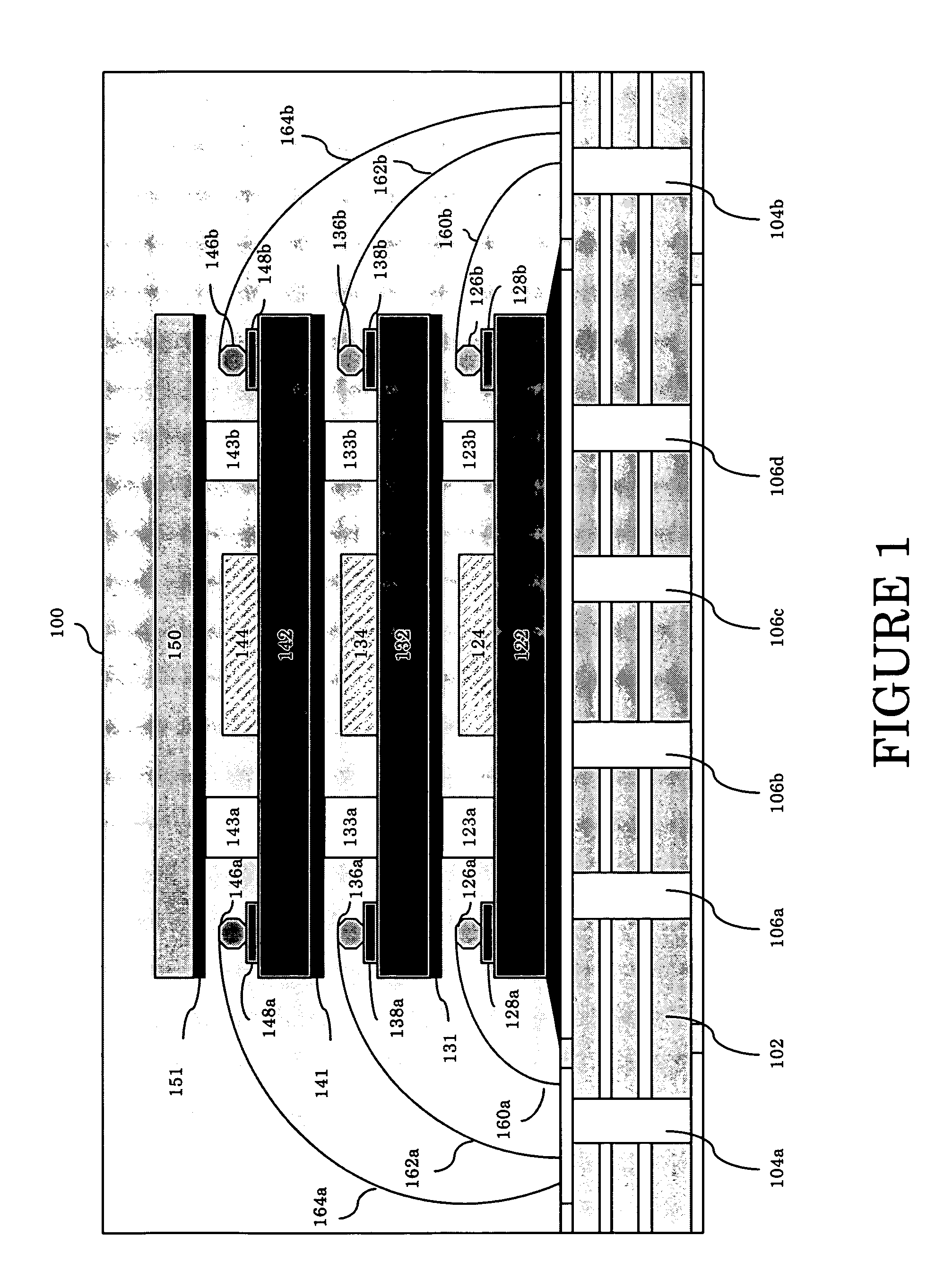
[0006]FIG. 1 illustrates an exemplary electronic module 100 in accordance with the present invention. The electronic module 100 includes a substrate 102 and two or more electronic devices, each of which comprise a wafer, active device, contact pads, and gold or copper balls. The substrate 102 includes one or more thermal vias 106a-106d, one or more input / output (I / O) lines 104a and 104b, and integrated transmission lines and inductors. Substrate 102 can be a lead free (LF) laminate or ceramic substrate.

[0007] A first electronic device includes a wafer 122, active device 124, gold or copper balls 126a and 126b, and contact pads 128a and 128b. The contact pads 128a and 128b are respectively coupled to the I / O lines 104a and 104b by bonding wires 160a and 160b.

[0008] A second electronic device is arranged on spacers 123a and 123b above the first electronic device, thereby forming a uniform and sealed air gap between the first and second electronic devices. Specifically, an adhesive l...


PUM


Abstract

An electronic module and a process for forming an electronic module are provided. Uniform and sealed air gaps are formed in a vertical direction between two or more electronic devices. The uniform and sealed air gaps are formed by arranging spacers between the electronic devices, where the height of the spacers is selected depending upon the operating characteristics of the particular type of electronic devices.

Description

BACKGROUND OF THE INVENTION [0001] Today's semiconductor packages include a number of different electronic devices. These electronic devices can include, for example, integrated circuits (ICs), microelectronic machines (MEMs), and / or the like. The integration of different electronic devices into a device module typically requires a significant amount of horizontal space, and relatively high assembly and processing complexity and cost. Current techniques for integrating different electronic devices into a device module largely focus on minimizing two-dimensional (X,Y) area of the discrete electronic devices. The discrete devices are assembled separately into the modules, where each such module includes a separate lid. Additionally, the assembled discrete devices occupy at least as much area in the two-dimensional (X,Y) portion of the module as the combined two-dimension area of the individual devices. SUMMARY OF THE INVENTION [0002] An electronic module and process for forming the sa...

Claims


Application Information

Patent Timeline
Patent Type & Authority Applications(United States)
IPC IPC(8): H05K7/00
CPCH01L25/0657H01L2224/32145H01L2924/1461H05K1/144H01L2924/30107H01L2924/16235H01L2924/16195H01L2924/09701H01L2924/01079H01L2225/06596H01L2225/06582H01L2225/06575H01L2225/06555H01L2224/48091H01L2224/48227H01L2224/48465H01L2225/0651H01L2225/06513H01L2225/06541H01L2924/00014H01L2924/00H01L23/12
Inventor WARREN, ROBERT W.LIANG, STEVE X.LOBIANCO, TONYGAN, GENE
Owner SKYWORKS SOLUTIONS INC
Why Eureka
Try Eureka