

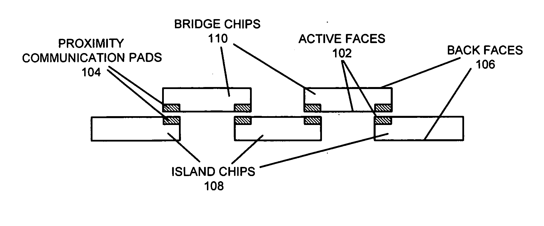
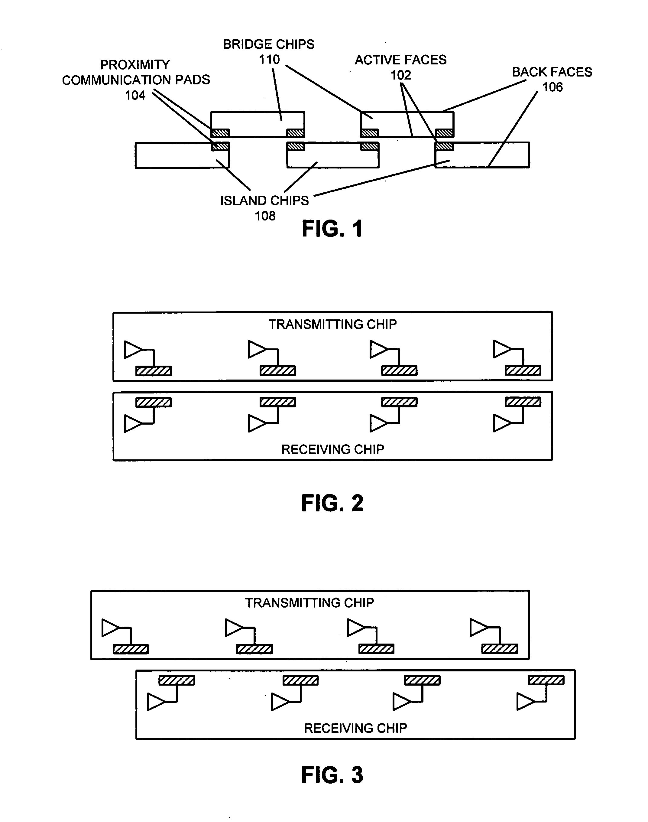
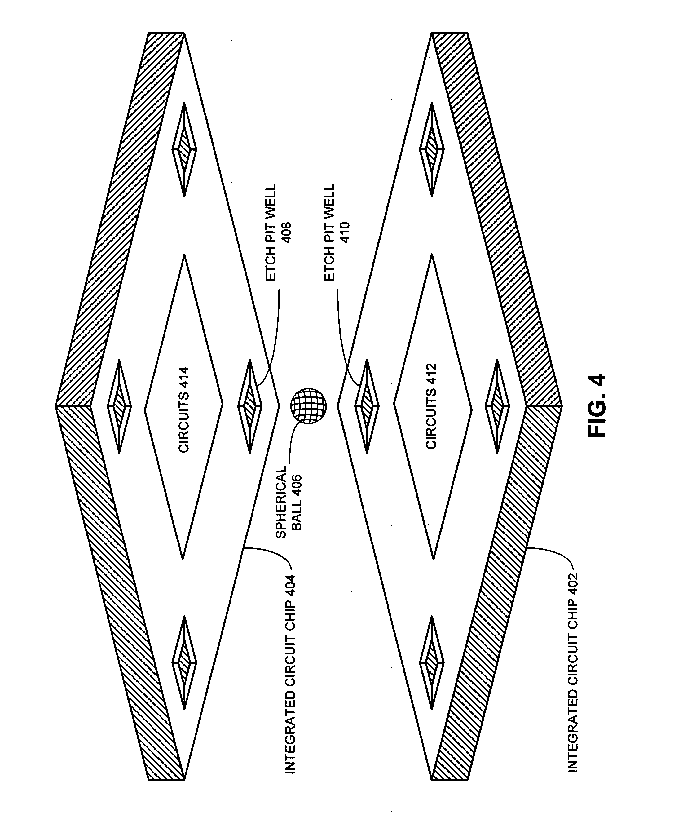
Method and apparatus for facilitating proximity communication and power delivery
a proximity communication and power delivery technology, applied in the field of assembly systems, can solve the problems of imposing pressure on the ability of resistive wires, introducing topological constraints, and challenging the achievement and maintenance of proximity communication chip alignments, and achieve the effect of facilitating precise inter-chip alignmen
- Summary
- Abstract
- Description
- Claims
- Application Information
AI Technical Summary
Benefits of technology
Problems solved by technology
Method used
Image

Examples
Embodiment Construction
[0027] The following description is presented to enable any person skilled in the art to make and use the invention, and is provided in the context of a particular application and its requirements. Various modifications to the disclosed embodiments will be readily apparent to those skilled in the art, and the general principles defined herein may be applied to other embodiments and applications without departing from the spirit and scope of the present invention. Thus, the present invention is not limited to the embodiments shown, but is to be accorded the widest scope consistent with the claims.
[0028] The data structures and code described in this detailed description are typically stored on a computer-readable storage medium, which may be any device or medium that can store code and / or data for use by a computer system. This includes, but is not limited to, magnetic and optical storage devices such as disk drives, magnetic tape, CDs (compact discs), DVDs (digital versatile discs ...
PUM
 Abstract
Description
Claims
Application Information