
Light modulation element and image display device

a light modulation element and image display technology, applied in non-linear optics, instruments, optics, etc., can solve the problems of high precision and high speed of modulation limit of these elements

Inactive Publication Date: 2007-04-05
FUJIFILM BUSINESS INNOVATION CORP
View PDF9 Cites 13 Cited by
  • Summary
  • Abstract
  • Description
  • Claims
  • Application Information

AI Technical Summary

Problems solved by technology

However, since there are limits to these elements with respect to high precision and high speed in the modulation, an element which optically conducts light modulation is gathering attention.

Method used


Image

  • Light modulation element and image display device
  • Light modulation element and image display device
  • Light modulation element and image display device

Examples


experimental example

[0094] In order to confirm the effect of the light modulation element of the invention, the following experiments are carried out. Specifically, light modulation elements with a light shielding layer and a liquid crystal layer are prepared and subjected to a heating and accelerating test so as to show change of the electric resistance of the liquid crystal contained in the liquid crystal layer. Furthermore, brief comparison of the characteristics of the light modulation elements is carried out.

Preparation of Light Modulation Element

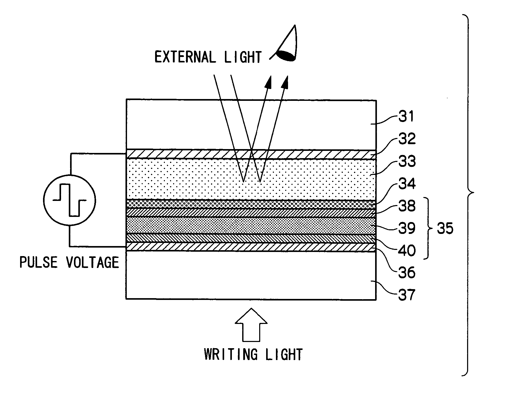
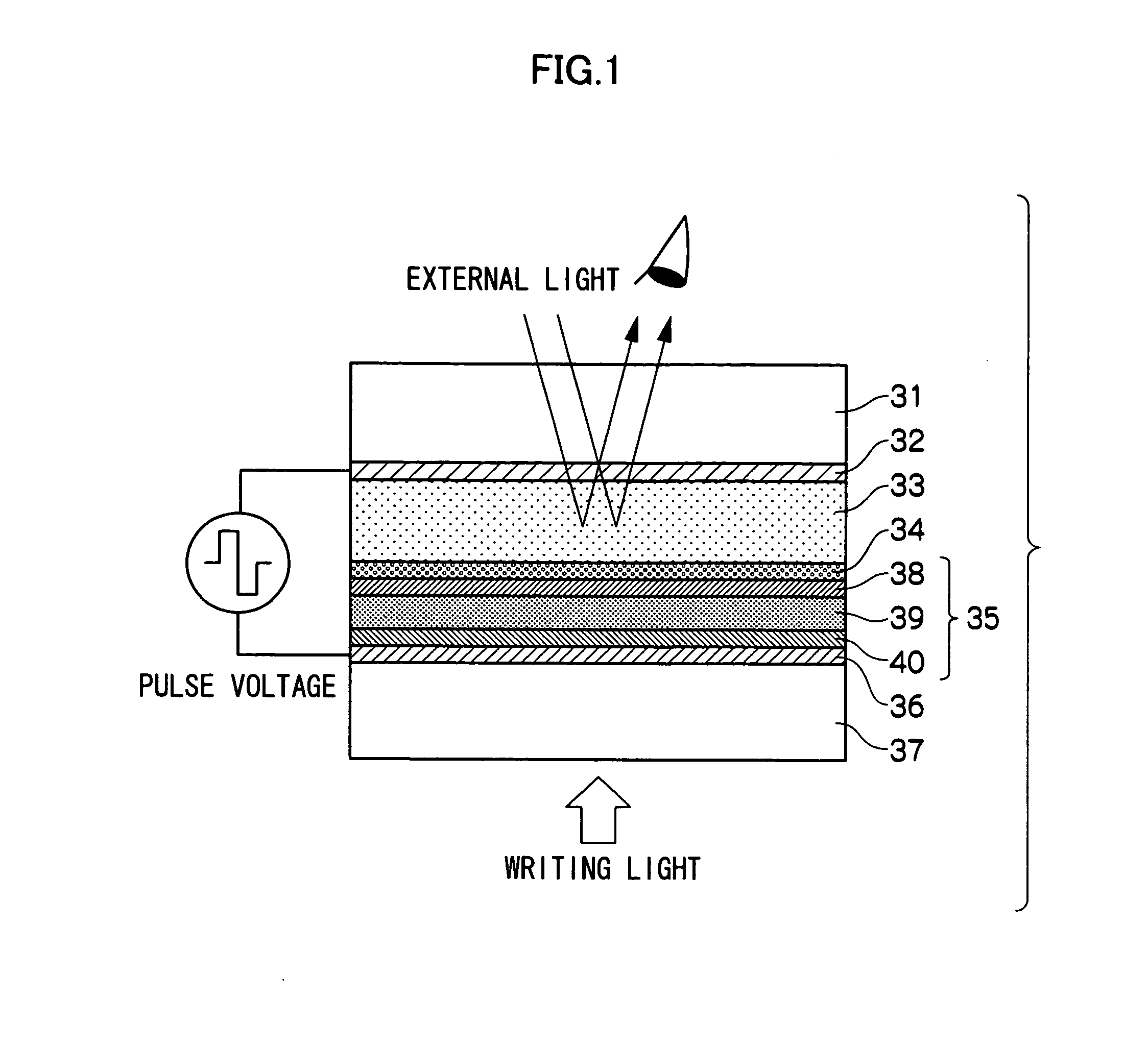
[0095] A light modulation element having the same structure as in FIG. 1 is prepared. Specifically, a commercially available PET resin film on one surface of which ITO is formed is used as a transparent substrate 37 (area of 85.5 mm×54 mm). An OPC layer 35 having a three-layered structure of a first charge-generating layer 40, a charge transport layer 39 and a second charge-generating layer 38 is formed on the transparent substrate 37 as follows.

[0096...


PUM


Abstract

The present invention provides a light modulation element in which a visible image is written by simultaneously conducting irradiation of the light modulation element with exposure light according to image information which corresponds to the visible image and application of a voltage, having: a pair of electrodes to which the voltage is applied; a photoconductive layer which, when the light modulation element has been irradiated with the exposure light, shows an electric characteristic distribution corresponding to the intensity distribution of the exposure light; a liquid crystal layer to which a partial voltage derived from the voltage applied to the pair of electrodes and having a distribution corresponding to the electric characteristic distribution of the photoconductive layer is applied to record a visible image having an optical characteristic distribution corresponding to the distribution of the partial voltage; and a light shielding layer disposed between the photoconductive layer and the liquid crystal layer, wherein the photoconductive layer, the liquid crystal layer and the light shielding layer are disposed between the electrodes, and the light shielding layer contains a resin including partially saponified polyvinyl alcohol; and an image display device including the same.

Description

CROSS-REFERENCE TO RELATED APPLICATION [0001] This application claims priority under 35 U.S.C. 119 from Japanese Patent Application No. 2005-291894, the disclosure of which is incorporated by reference herein. TECHNICAL FIELD [0002] The invention relates to a light modulation element having a photoconductive layer, a light shielding layer and a liquid crystal layer which are laminated, and to an image display device including the same. RELATED ART [0003] Light modulation elements that make use of the electro-optic effect, the magneto-optic effect or the acousto-optic effect are conventionally known. However, since there are limits to these elements with respect to high precision and high speed in the modulation, an element which optically conducts light modulation is gathering attention. As an element that optically conducts light modulation, an element having a combination of a photoconductive layer and a liquid crystal layer and an element including a mixture of a ferroelectric li...

Claims


Application Information

Patent Timeline
IPC IPC(8): G02F1/135
CPCG02F1/135G02F2001/1351G02F1/1351
Inventor GOMYOU, MAKOTOHARADA, HARUOOKANO, YASUNORIGAN, TAIJYUARISAWA, HIROSHI
Owner FUJIFILM BUSINESS INNOVATION CORP
Learn More