Light emitting device and manufacturing method thereof

a technology of light emitting devices and manufacturing methods, applied in the direction of semiconductor devices, basic electric elements, electrical appliances, etc., can solve the problems of reducing the number of holes injected, deterioration of the light emitting element itself, and the number of holes

Inactive Publication Date: 2004-04-13
SEMICON ENERGY LAB CO LTD
View PDF26 Cites 88 Cited by
  • Summary
  • Abstract
  • Description
  • Claims
  • Application Information

AI Technical Summary

Problems solved by technology

The anode is an electrode for injecting holes that participate in light emission in the organic compound layer, and it is thought that cracks developing in the anode may adversely influence the generation of holes, may reduce the number of holes injected, and in addition, may become a cause of deterioration of the light emitting element itself.
Roughness on an anode surface is thought to exert an adverse influence on the generation and injection of holes, to reduce the number of holes injected, and to cause deterioration of the light emitting element itself due to cracks.
In addition, the organic compound layers easily deteriorate due to oxygen and moisture, and organic resin materials such as polyimide, polyamide, and acrylic are often used as interlayer insulating films.
There is a problem in that the light emitting elements deteriorate due to gases such as oxygen generated from interlayer insulating films formed by the aforementioned materials.

Method used


Image

  • Light emitting device and manufacturing method thereof
  • Light emitting device and manufacturing method thereof
  • Light emitting device and manufacturing method thereof

Examples


embodiment 1

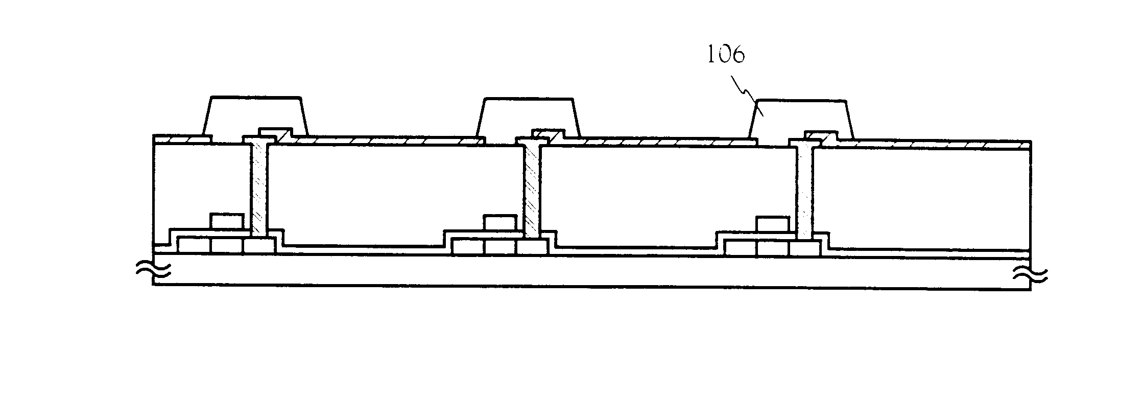
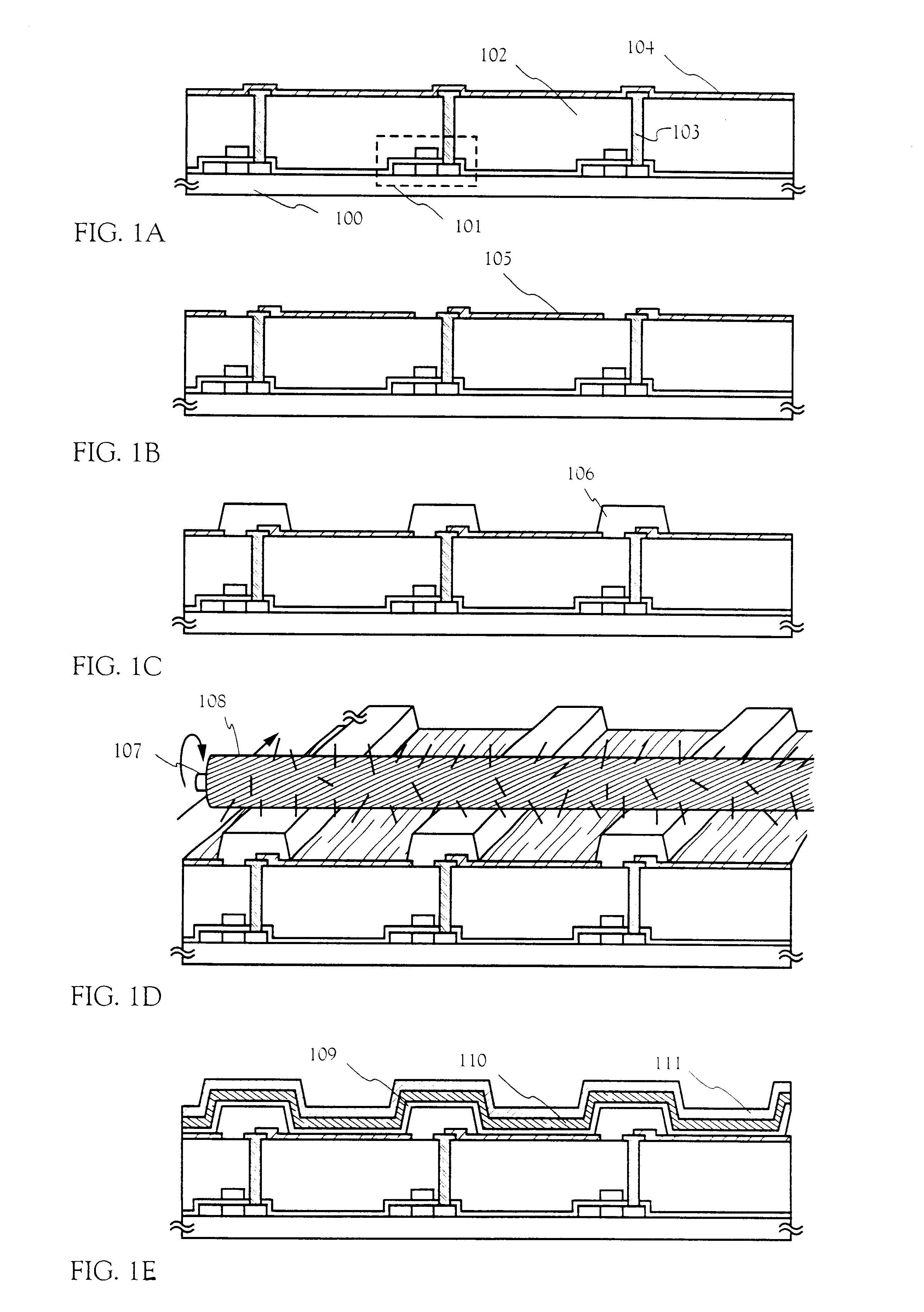
In this embodiment, the light emitting element formed by using the present invention is explained. Described next is an example of a method of manufacturing, at the same time over the same substrate, TFTs for a pixel portion having an organic light emitting element of the present invention and TFTs (an n-channel TFT and a p-channel TFT) for a driver circuit that is provided in the periphery of the pixel portion. The description will be given with reference to FIGS. 3A to 6C.

First, this embodiment uses a substrate 900 made of barium borosilicate glass, typically Corning #7059 glass and # 1737 glass (products of Corning Incorporated), or alumino borosilicate glass. No limitation is put to the material of the substrate 900 as long as it is light-transmissive (translucent), and a quartz substrate may be used. A plastic substrate may also be used if it can withstand heat at the process temperature of this embodiment.

Next, as shown in FIG. 3A, a base film 901 is formed on the substrate 90...

embodiment 2

A method of manufacturing a light emitting device is explained in Embodiment 2 using FIGS. 18 to 21B by taking an example different from that in Embodiment 1.

Manufacturing is performed in accordance with Embodiment 1 up through the step of forming the two layer conductive films 907 and 908 on the gate insulating film 906, as shown in FIG. 3A.

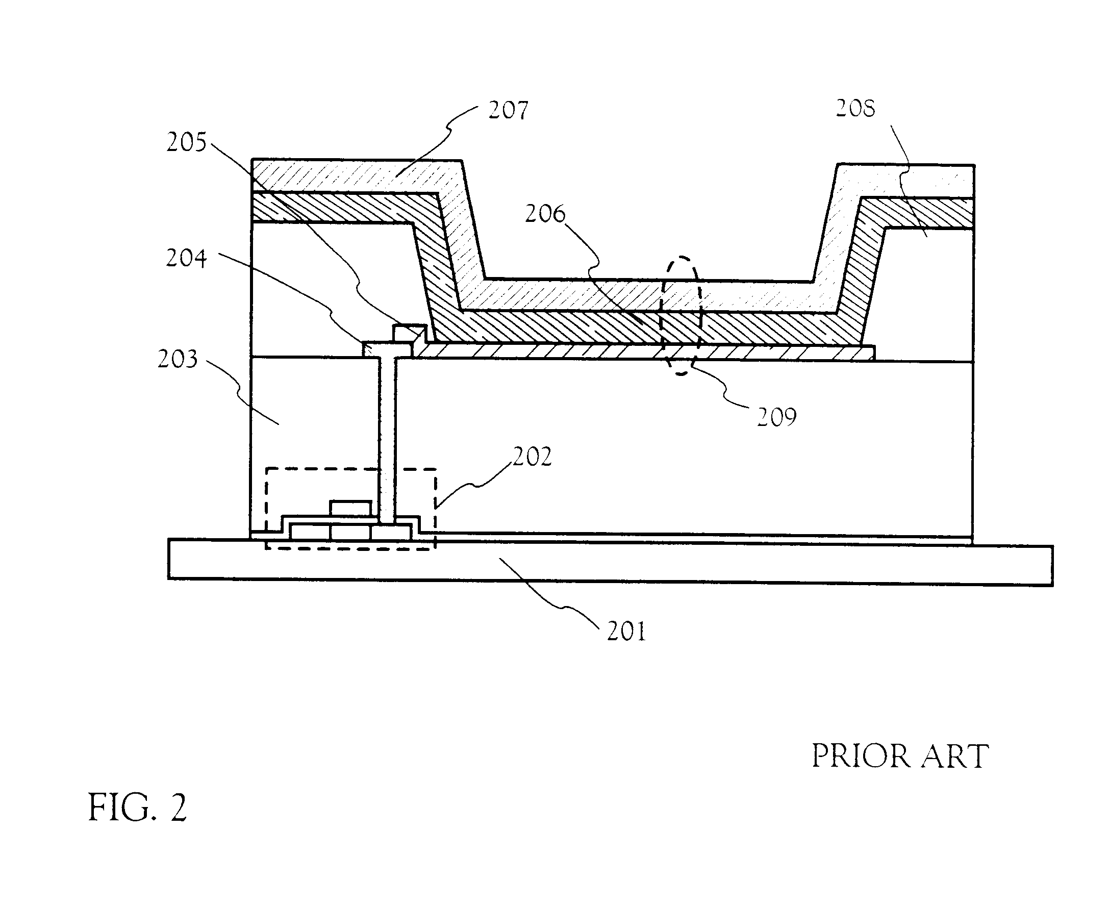
The conductive films 907 and 908 are then etched using the masks 909a to 909d, forming conductive layers 3901 to 3904 (3901a-3904a and 3901b-3904b) having a first tapered shape. An ICP (inductively coupled plasma) etching method is used for the etching. There are no limitations placed on the etching gasses used, but CF.sub.4, Cl.sub.2, and O.sub.2 are used for etching of the W film and tantalum nitride film. The gas flow rates are set so as to be 25:25:10, respectively, and etching is performed at a pressure of 1 Pa with an RF (13.56 MHz) electric power of 500 W introduced into a coil shape electrode. An RF (13.56 MHz) electric power of 150 W is...

embodiment 3

can be used in combination with the embodiment mode and Embodiments 1 and 2.


PUM

PropertyMeasurementUnit
band gapaaaaaaaaaa
thicknessaaaaaaaaaa
transparentaaaaaaaaaa

Abstract

A method of manufacturing a high quality light emitting device is provided, in which light emitting elements having long life are manufactured by using light emitting elements having a structure that deteriorates less easily than conventional structures. After forming a bank, an exposed anode surface is wiped using a PVA (polyvinyl alcohol)-based porous medium, performing leveling and removal of debris. An insulating film is formed covering the bank and the anode, unevenness on the anode surface is covered, and the balance between the amount of holes and electrons injected into an organic compound layer can be regulated.

Description

1. Field of the InventionThe present invention relates to a light emitting device using a light emitting element with a film containing an organic compound that emits light with application of electric field (hereinafter referred to as organic compound layer), as well as an anode and a cathode. Specifically, the present invention relates to a light emitting device using a light emitting element with lower drive voltage than before and longer lifetime. The term "light emitting device" in this specification refers to an image display device or a light emitting device that employs as a light emitting element a light emitting element. Also included in the definition of the light emitting device are a module in which a connector, such as an anisotropic conductive film (FPC: flexible printed circuit), a TAB (tape automated bonding) tape, or a TCP (tape carrier package), is attached to an organic light emitting element, a module in which a printed wiring board is provided on the tip of a T...

Claims


Application Information

Patent Timeline
Patent Type & Authority Patents(United States)
IPC IPC(8): H01L27/32H01L51/50H01L27/28H01L51/52H01L51/56
CPCH01L27/3246H01L51/50H01L51/5206H01L27/3258H01L51/5237H01L51/56H10K59/124H10K59/122H10K50/00H10K50/81H10K50/841H10K2101/00H10K71/00
Inventor YAMAGATA, HIROKAZUYAMAZAKI, SHUNPEITAKAYAMA, TORU
Owner SEMICON ENERGY LAB CO LTD
Why Eureka
Try Eureka