

Clock circuit for semiconductor memories
Inactive Publication Date: 2007-04-26
POLARIS INNOVATIONS
View PDF3 Cites 12 Cited by
- Summary
- Abstract
- Description
- Claims
- Application Information
AI Technical Summary
Benefits of technology
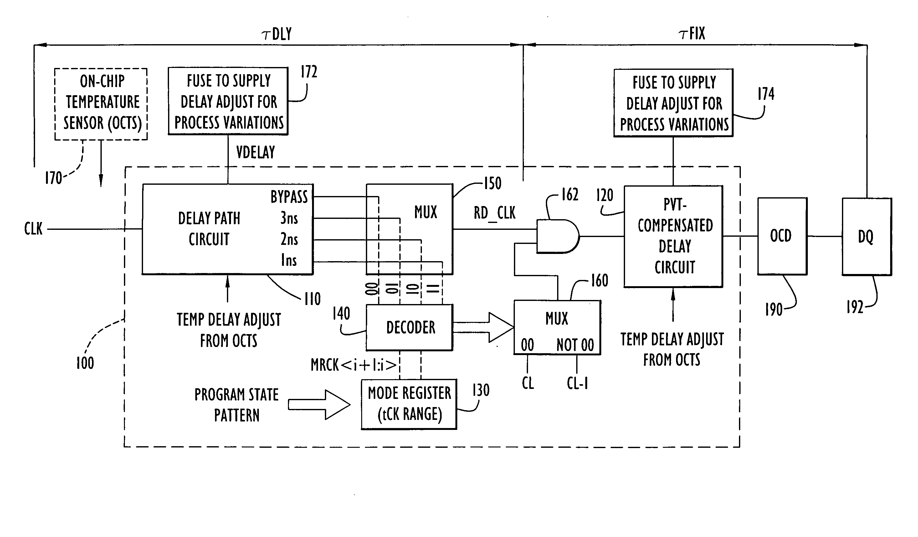
[0006] A circuit and method for producing a read clock signal in a semiconductor memory device from an input clock signal to ensure that the read access time does not exceed the clock cycle time. When producing the read clock signal, one of a plurality of delay amounts is selected to be
Problems solved by technology
It is very difficult to significantly improve tAC.
However, as clock signal frequencies become faster with improving semiconductor technologies, the clock cycle time (tCK) will become so small that tAC may exceed tCK.
A DLL circuit may consume a few milliamps (mA) even when the host device is in stand-by mode if the clock is running.
A DLL circuit is rarely used in semiconductor devices for low power applications because the DLL power consumption even in a stand-by mode may quickly deplete the battery of the system.
Method used
View moreImage
Smart ImageViewing Examples

Examples
case 1
[0028] When tCK is 5 ns, then the selected internal delay τDLY is 0, such that tAC is 4 ns (which is less than tCK of 5 ns).
case 2
[0029] When tCK is 4 ns, then the selected internal delay τDLY is 3 ns, such that tAC is 3 ns (which is less than tCK of 4 ns).
case 3
[0030] When tCK is 3.5 ns, then τDLY is 2 ns such that tAC is 2.5 ns, (which is less than tCK of 3.5 ns).
Login to View More PUM
 Abstract
A circuit and method for producing a read clock signal in a semiconductor memory device from an input clock signal to ensure that the read access time does not exceed the clock cycle time. One of a plurality of delay amounts is selected to be imposed on the input clock signal depending on the frequency of the clock signal.
Description
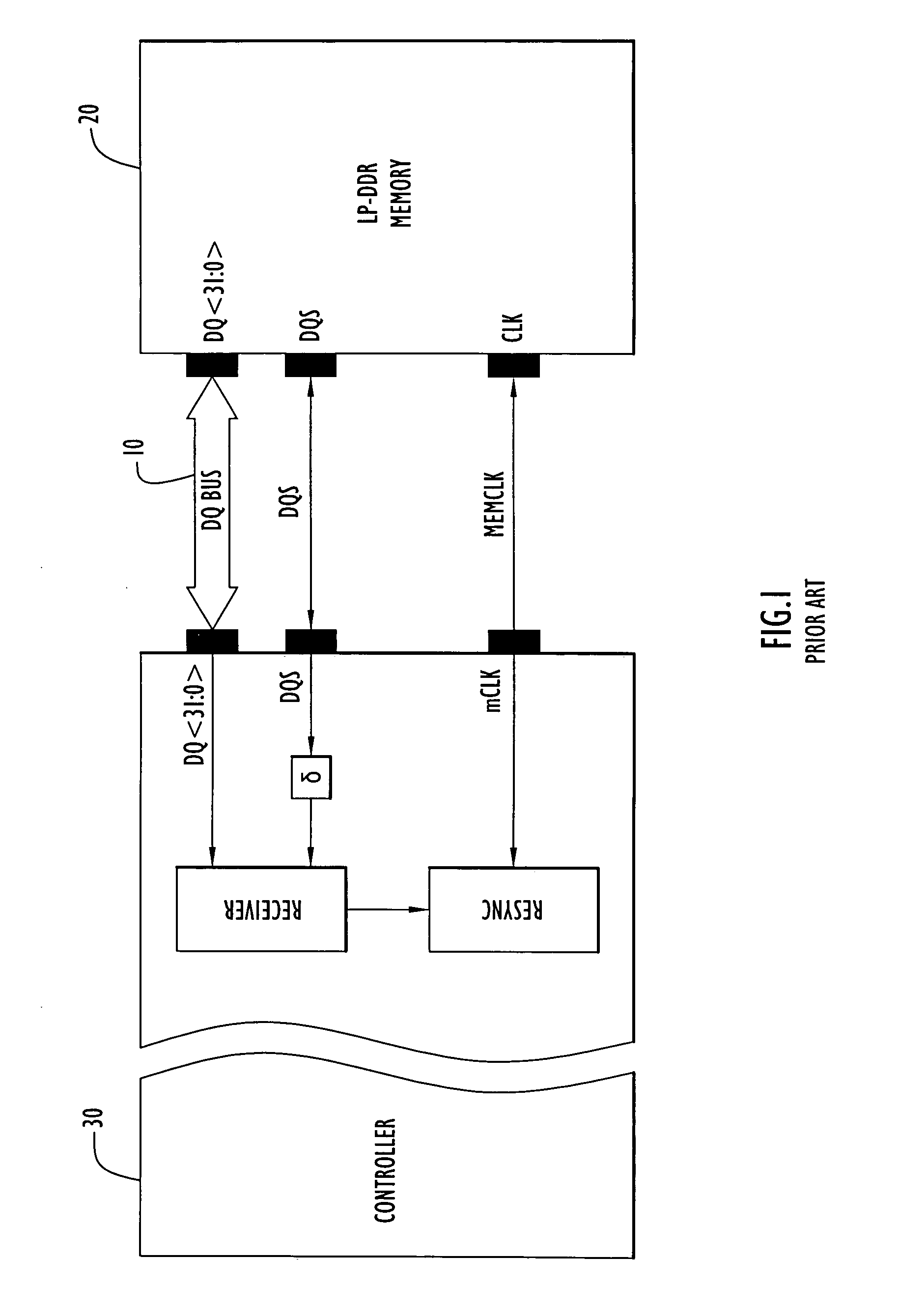
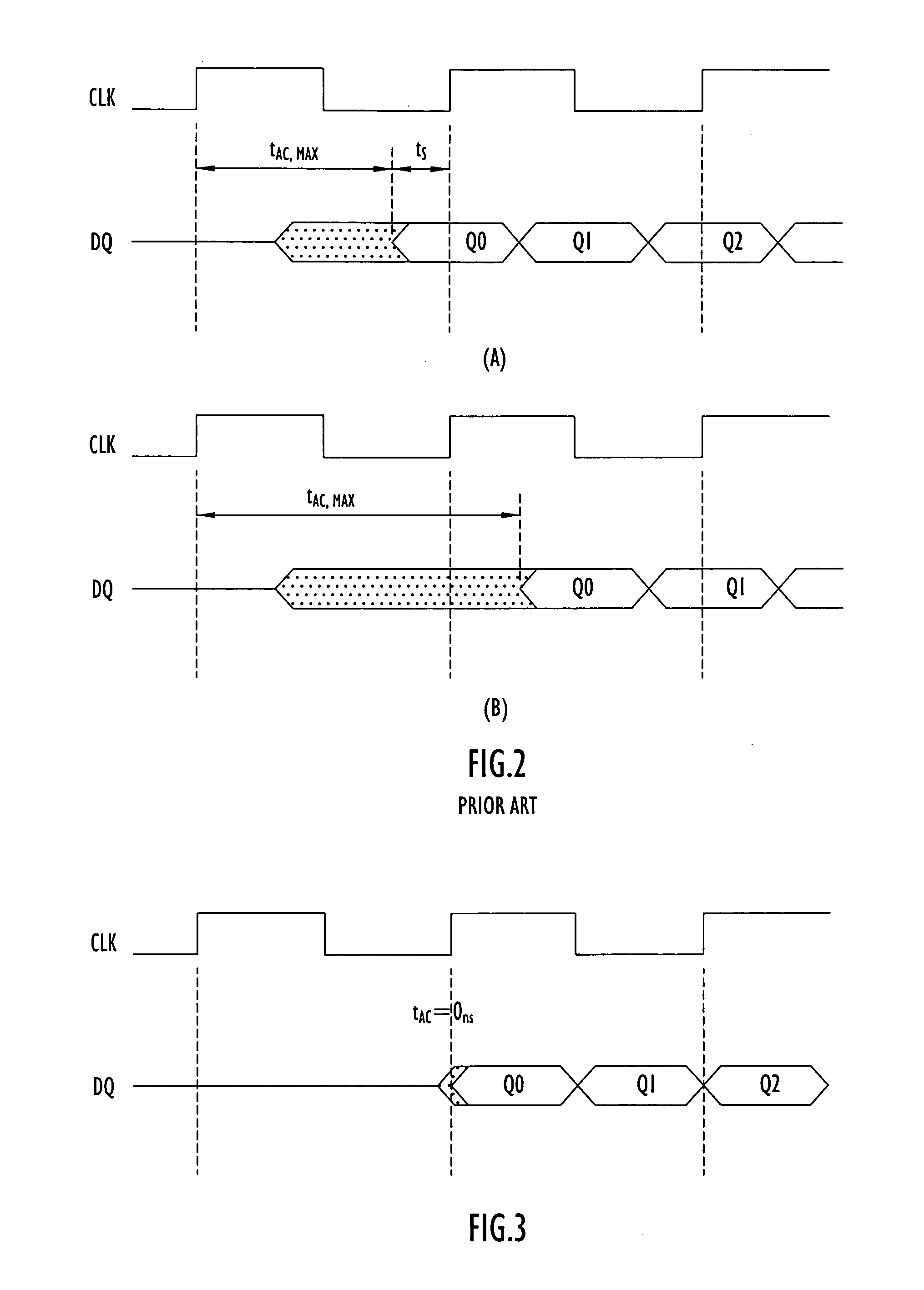
BACKGROUND OF THE INVENTION [0001] The present invention is directed to semiconductor devices, and more particularly to a clock circuit for semiconductor memory devices. [0002]FIG. 1 shows an exemplary memory interface in a low-power synchronous dynamic random access memory (SDRAM) device. A data bus (DQ bus) 10 is interfaced between an LP-DDR memory chip 20 and a controller 30. The controller 30 generates a memory clock (MemCLK) signal that is connected to the CLK input of the memory chip 20. In low-power semiconductor devices, such as low power-single data rate (LP-SDR) or low power-double data rate (LP-DDR) SDRAM devices, the read access to load valid data onto the data bus 10 is triggered by clock edges of the MemCLK signal. The [0003] Turning to FIGS. 2(A) and 2(B), there is a read access time (tAC) that results from an intrinsic delay path as shown with respect to the main clock signal (CLK). It is very difficult to significantly improve tAC. The controller 30 can sample and r...
Claims
Login to View More Application Information
Patent Timeline
 IPC IPC(8): G11C8/00
CPCG11C7/04G11C7/22G11C7/222G11C11/419G11C11/40626G11C11/4076G11C2207/2254
InventorOH, JONG-HOON
OwnerPOLARIS INNOVATIONS