Methods and apparatus for assembling a printed circuit board

a printed circuit board and assembly method technology, applied in the field of printed circuit boards, can solve the problems of increasing the maintenance cost of equipment utilizing such electrical components, reducing the operation reliability of electrical components,

Active Publication Date: 2007-05-03
HAIER US APPLIANCE SOLUTIONS INC
View PDF8 Cites 21 Cited by
  • Summary
  • Abstract
  • Description
  • Claims
  • Application Information

AI Technical Summary

Problems solved by technology

Such tin whiskers considerably decrease the operation reliability of the electrical components, and increase the maintenance cost of the equipment utilizing such electrical components.
At least some known producers store the wave soldered components for 3000 to 4000 hours for observing the tin whisker situation, which is obviously undesired by the producers.

Method used


Image

  • Methods and apparatus for assembling a printed circuit board
  • Methods and apparatus for assembling a printed circuit board
  • Methods and apparatus for assembling a printed circuit board

Examples


Embodiment Construction

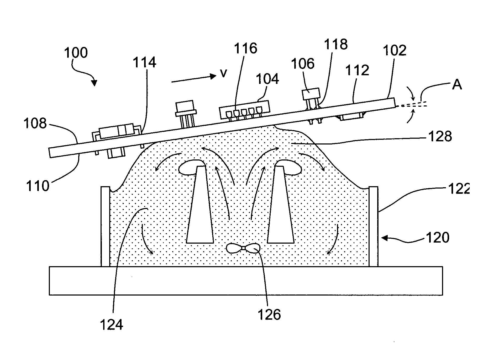
[0013]FIG. 1 illustrates an exemplary printed circuit board (PCB) 100 applicable to the present invention. PCB 100 includes a board 102, a plurality of surface mount electrical components 104 mounted on board 102, and a plurality of through-hole mount electrical components 106 mounted on board 102.

[0014] In the exemplary embodiment, board 102 includes a first surface 108 and a second surface 110 opposite first surface 108 for mounting electrical components 104, 106 thereon. Board 102 also includes a plurality of electrical traces 112 defined on first and second surfaces 108, 110, and a plurality of through holes 114 defined therethrough for mounting through-hole mount components 106.

[0015] In the exemplary embodiment, each surface mount component 104 includes a plurality of electrical terminals 116 for being positioned on or adjacent board 102. Each through-hole mount component 106 also includes a plurality of electrical terminals 118 for inserting into through holes 114 of board ...


PUM

PropertyMeasurementUnit
angleaaaaaaaaaa
angleaaaaaaaaaa
angleaaaaaaaaaa

Abstract

A method for manufacturing a printed circuit board includes providing a board including a plurality of electrical traces, a first surface, and a second surface opposite the first surface. The method further includes providing at least one surface mount component having a plurality of electrical terminals. The method also includes applying an adhesive on the first surface of the board, and adhering the surface mounting component to the first surface. The method also includes wave soldering the surface mount component on the first surface to the board to encapsulate at least a portion of the electrical terminals of the surface mount component with a lead-free solder.

Description

BACKGROUND OF THE INVENTION [0001] This invention relates generally to printed circuit boards, and, more particularly, to methods and apparatus for soldering printed circuit boards. [0002] Tin or tin alloy deposits have been widely used in fabricating electronic circuits, electronic devices and electrical connectors because of the benefits that such deposits provide. For example, tin and tin alloy deposits protect the components from corrosion, provide a chemically stable surface for soldering and maintain good surface electrical contact. [0003] At least some known electrical components, such as for example, surface mount components have a plurality of conductive terminals with tin or tin alloy deposit thereon. The terminals of the surface mount components are then placed on a printed circuit board, and are soldered onto the printed circuit board by a known reflow soldering process. However, most portion of the terminals are still exposed in the air after the reflow soldering proces...

Claims


Application Information

Patent Timeline
Patent Type & Authority Applications(United States)
IPC IPC(8): B23K31/02
CPCB23K1/085B23K2201/42H05K3/305H05K3/3415H05K3/3421Y10T29/49146H05K3/3463H05K3/3468H05K2203/1476H05K2203/1572H05K3/3447B23K2101/42Y02P70/50
Inventor HOLMES, JOHN S.
Owner HAIER US APPLIANCE SOLUTIONS INC
Why Eureka
Try Eureka