Electronic-part built-in substrate and manufacturing method therefor

a technology of built-in substrates and electronic components, which is applied in the direction of printed circuit manufacturing, printed circuit aspects, printed circuit non-printed electric components association, etc., can solve the problem that the heat generated from the bare chip 203/b> cannot be sufficiently radiated, and achieve the effect of enhancing the yield and efficiently radiating hea

Inactive Publication Date: 2007-05-03
SHINKO ELECTRIC IND CO LTD
View PDF10 Cites 121 Cited by
  • Summary
  • Abstract
  • Description
  • Claims
  • Application Information

AI Technical Summary

Benefits of technology

[0016] Embodiments of the present invention provide an electronic-part built-in substrate enabled to

Problems solved by technology

Therefore, the related art has another problem that heat gene

Method used


Image

  • Electronic-part built-in substrate and manufacturing method therefor
  • Electronic-part built-in substrate and manufacturing method therefor
  • Electronic-part built-in substrate and manufacturing method therefor

Examples


Embodiment Construction

[0059] Preferred embodiments of the present invention will hereinafter be described in detail with reference to the accompanying drawings.

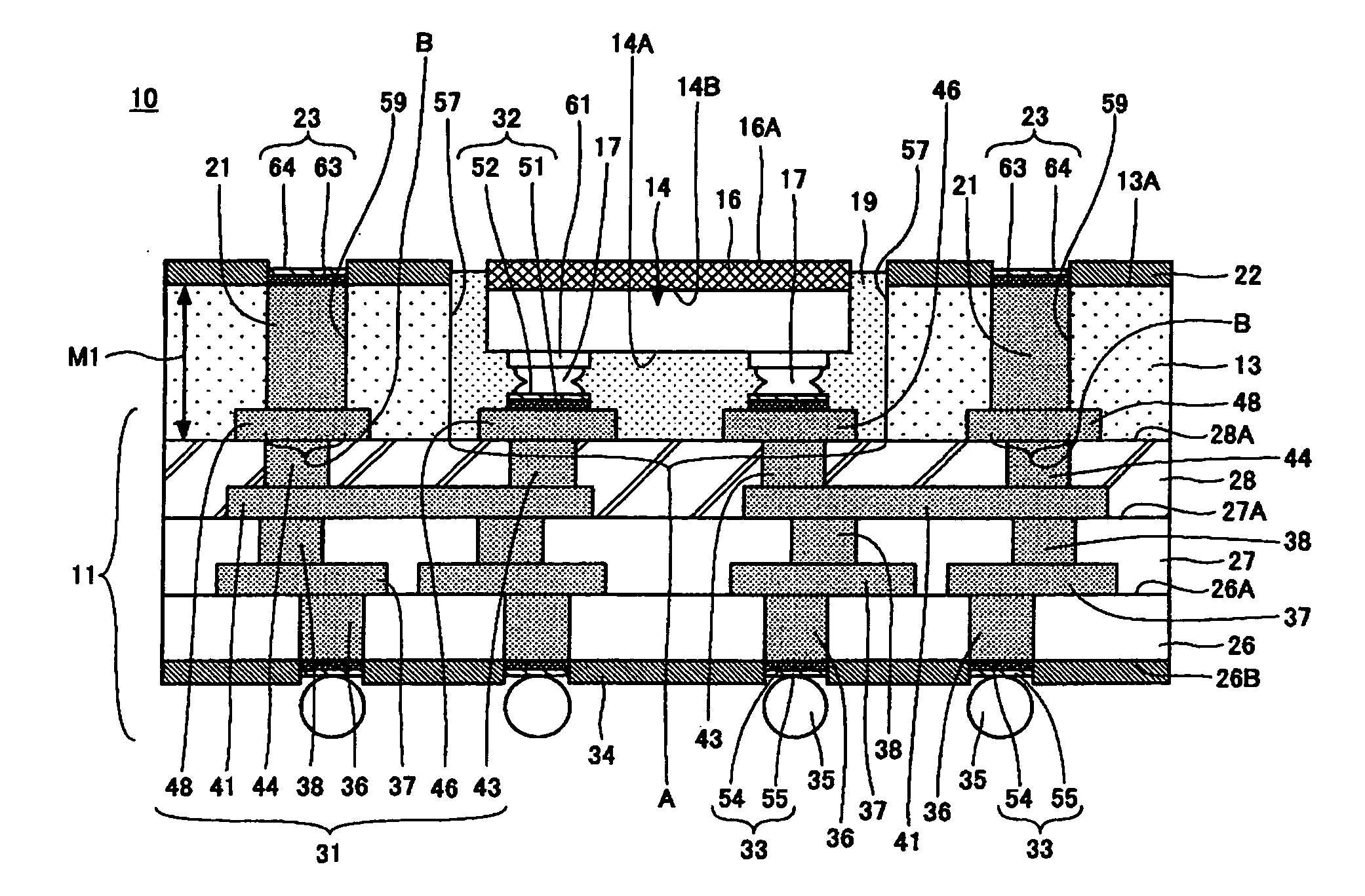
[0060]FIG. 1 is a cross-sectional view of an electronic-part built-in substrate according to the embodiment of the invention. In FIG. 1, reference character A denotes a region on a surface of the coreless substrate 11, in which a semiconductor chip 14 is connected (hereunder referred to as a “semiconductor chip connection region A”) . Reference character B denotes a position where a through-via 21 is formed (hereunder referred to as a “through-via formation position B”). Reference character M1 denotes a thickness of a resin layer 13 with respect to a top surface 28A of a prepreg resin layer 28 (hereunder referred to as a “thickness M1”). Incidentally, a case where the semiconductor chip 14 is built into the electronic-part built-in substrate as an electronic part will be described below as an example of the present embodiment of the invention.

[0...


PUM


Abstract

The electronic-part built-in substrate includes a coreless substrate 11 in which a wiring pattern 31 is formed in laminated insulating layers 26 and 27, a semiconductor chip 14 electrically connected to the wiring pattern 31, a resin layer 13 configured to cover a first main surface of the coreless substrate 11 and to have an accommodating portion 57 that accommodates the semiconductor chip 14, and a sealing resin 19 that seals the semiconductor chip 14 accommodated in the accommodating portion 57.

Description

[0001] This application claims foreign priority based on Japanese Patent application No. 2005-313243, filed Oct. 27, 2005, the content of which is incorporated herein by reference in its entirety. BACKGROUND OF THE INVENTION [0002] 1. Field of the Invention [0003] The present disclosure relates to an electronic part built-in substrate. In particular, the present disclosure relates to an electronic part built-in substrate having a multilayer wiring structure and an electronic part electrically connected to a wiring pattern provided in the multilayer wiring structure. [0004] 2. Description of the Related Art [0005] In recent years, significant progress has been made in high densification of electronic part, such as semiconductor chips, to thereby achieve the miniaturization thereof. Along with this, an electronic part built-in substrate has been proposed, which incorporates electronic part in a multilayer wiring structure configured so that a wiring pattern is formed in a plurality of...

Claims


Application Information

Patent Timeline
IPC IPC(8): H01L23/12
CPCH01L21/4857H01L23/3677H01L23/5389H01L24/81H01L25/0657H01L25/105H01L2221/68345H01L2224/13144H01L2224/16225H01L2224/32145H01L2224/32225H01L2224/48091H01L2224/48225H01L2224/48227H01L2224/73265H01L2224/81001H01L2224/81801H01L2224/82H01L2224/85H01L2224/86H01L2225/06568H01L2924/01078H01L2924/01079H01L2924/15153H01L2924/1517H01L2924/15311H01L2924/1532H01L2924/19041H01L2924/19105H05K3/4682H05K3/4697H05K2201/10674H01L24/48H01L2924/3511H01L2225/1058H01L2224/73204H01L2924/18161H01L2224/16235H01L2924/00014H01L2924/00H01L2924/00012H01L2924/12042H01L24/73H01L2224/05573H01L2224/05568H01L2924/181H01L2224/45099H01L2224/45015H01L2924/207H05K1/18
Inventor MACHIDA, YOSHIHIRO
Owner SHINKO ELECTRIC IND CO LTD
Why Eureka
Try Eureka