Eureka AIR delivers breakthrough ideas for toughest innovation challenges, trusted by R&D personnel around the world.

Self-mode-locked semiconductor laser

Inactive Publication Date: 2007-05-03
LUCENT TECH INC
View PDF4 Cites 11 Cited by
  • Summary
  • Abstract
  • Description
  • Claims
  • Application Information

AI Technical Summary

Benefits of technology

[0003] In accordance with the present invention, an interband self-mode-locked (SML) semiconductor laser utilizes an active waveguide structure that includes an active waveguide section and one or more passive waveguide sections that together enhances self-mode-locking. This scheme modifies minimally the laser diode fabrication process and provides shorter limits on laser cavity length, and therefore it pushes the limits on the pulse repetition rate. In one embodiment, a 1.56 um self-mode-locked semiconductor lasers operates at a 40 GHz repetition rate. The SML laser is based on enhanced Kerr lens mode-locking by vertically combining the active section with one or more passive waveguide sections. The full-width-half-maximum (FWHM) width of the pulse spectrum is over 8 nm and the time domain pulse duration is about 10 ps. The average output power coupled to a cleaved fiber is over 0 dBm.

Problems solved by technology

However, the inherent self-mode-locking effect in semiconductor lasers at 1.55 um, which involves interband transitions rather than intersubband transitions, is much weaker.

Method used


Image

  • Self-mode-locked semiconductor laser
  • Self-mode-locked semiconductor laser
  • Self-mode-locked semiconductor laser

Examples


Embodiment Construction

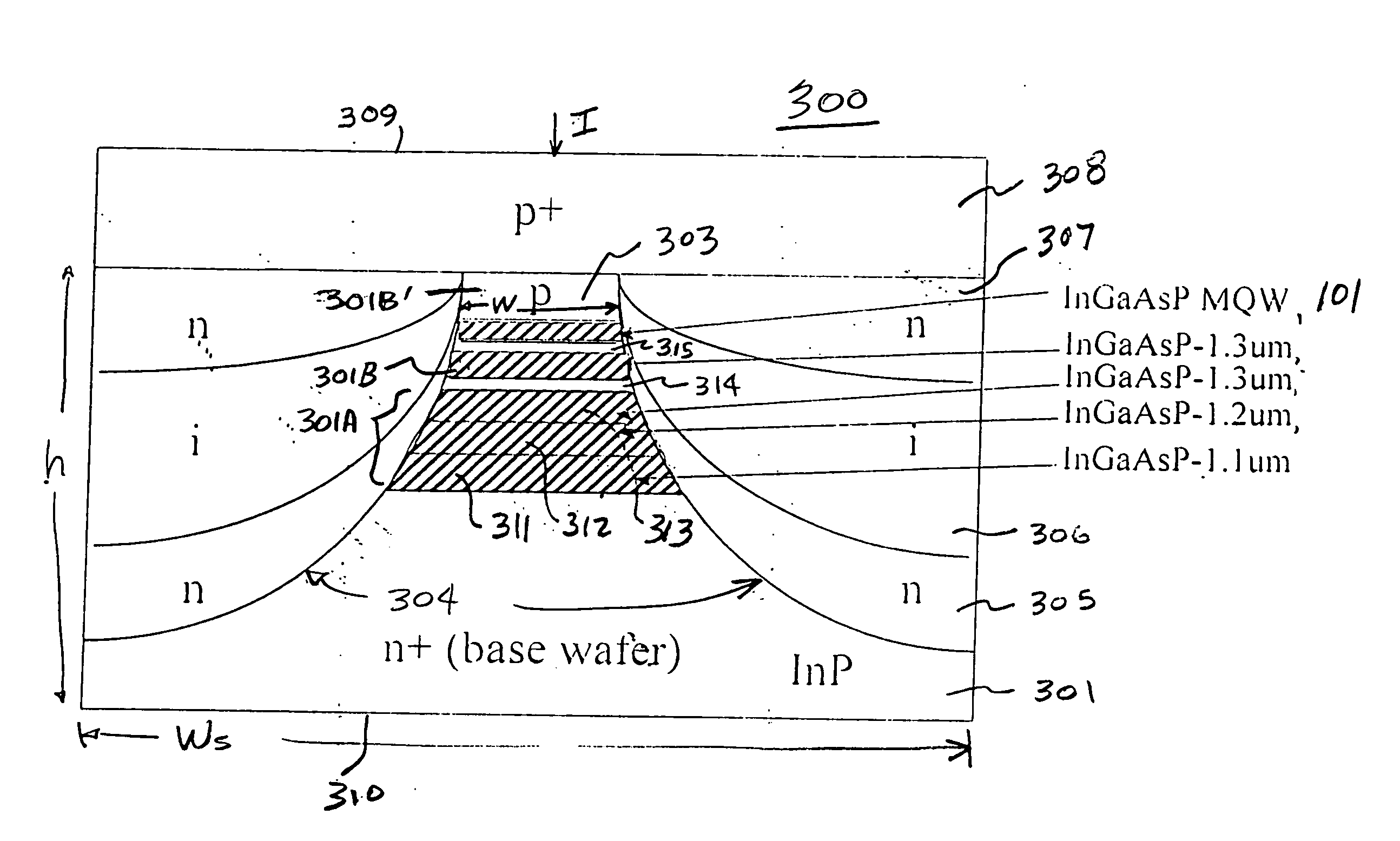
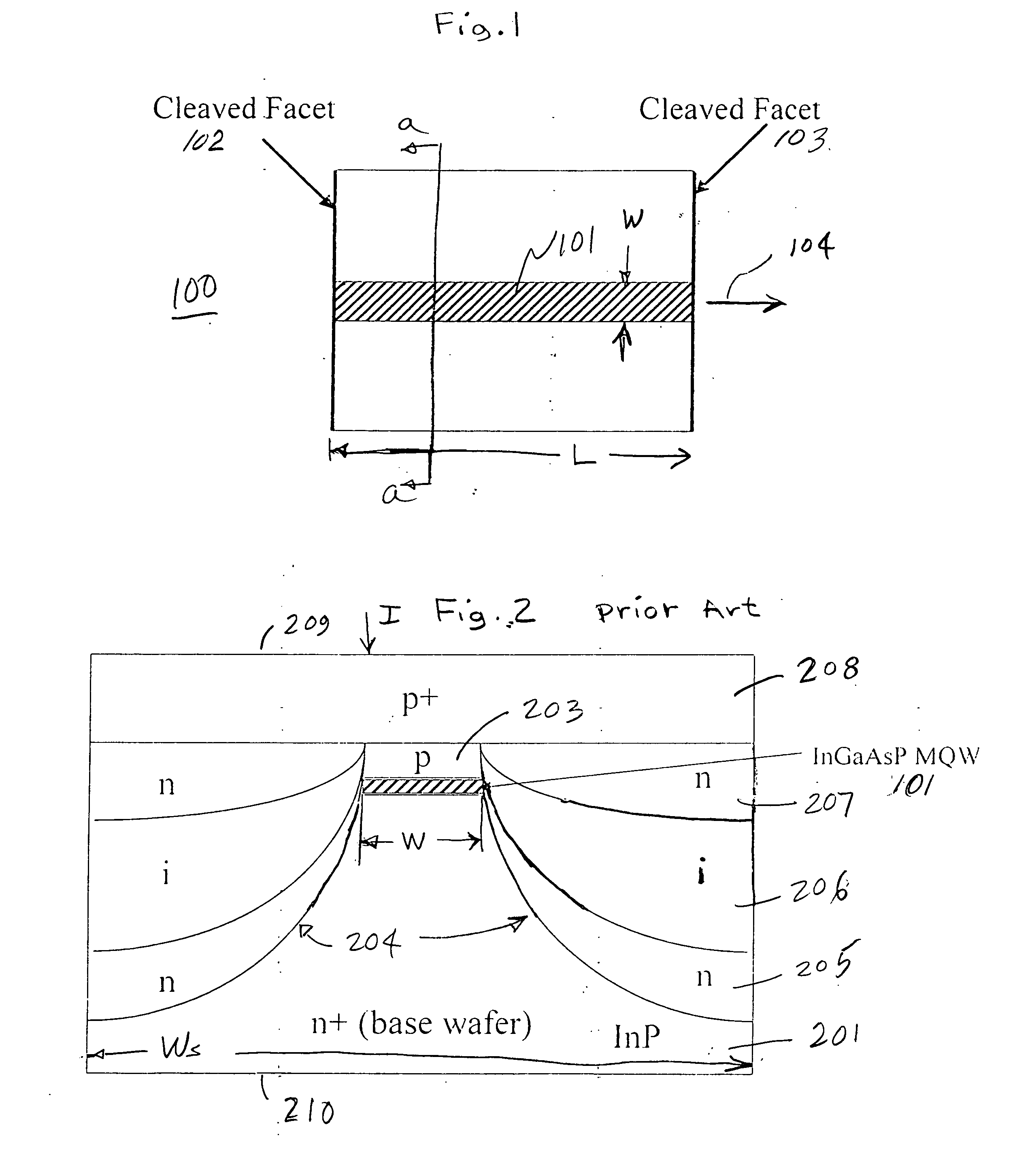
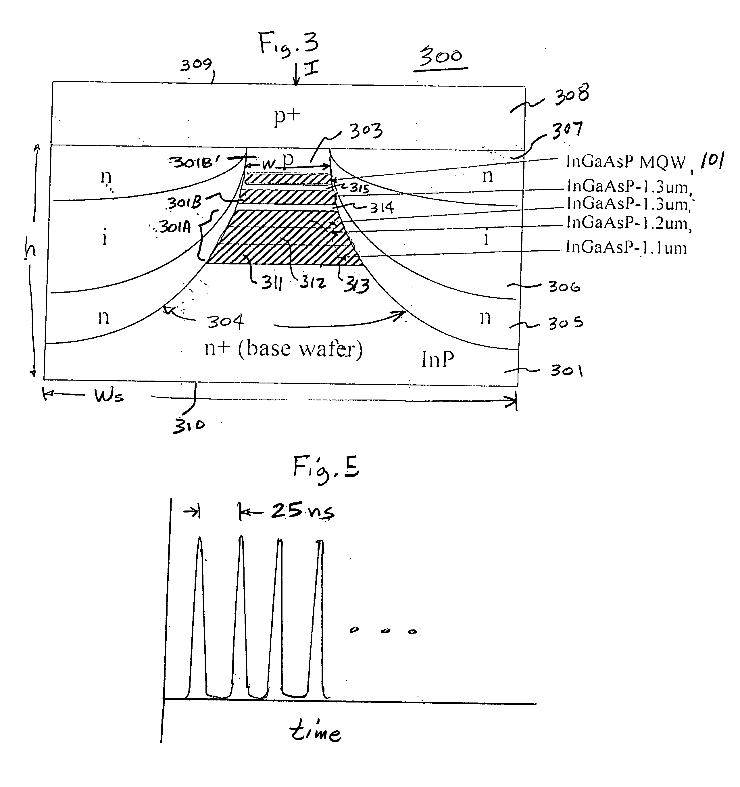
[0017] With reference to FIG. 1 there is shown a top view of a prior art edge-emitting index-guided semiconductor laser 100. The shaded area indicates the active waveguide 101. In the prior art such a laser was fabricated as an interband continuous wave (CW) laser or as an intersubband self-start self-mode locked (SML) laser. The laser cavity L is formed by two cleaved facets 102 and 103 and the laser frequency is determined by the length of cavity and the index of refraction of the waveguide. The cleaving of laser 100 is done after the laser 100 has been completely fabricated as will be discussed with reference to FIG. 2. The output of the edge-emitting laser 100 is emitted from the active multiple quantum wells (MQW) region and is shown by 104.

[0018] With reference to FIG. 2 there is shown an illustrative cross-section view of section a-a of FIG. 1. The CW laser 100 can be fabricated using a ridge-waveguide structure for weak index guiding or an etched-mesa for strong index guidi...


PUM


Abstract

An interband self-mode-locked (SML) semiconductor laser utilizes an active waveguide structure that includes an active waveguide section and one or more passive waveguide sections that together enhances self-mode-locking. The SML laser operation is based on enhanced Kerr lens mode-locking by vertically optically combining the active section with one or more passive waveguide sections.

Description

FIELD OF THE INVENTION [0001] The present invention relates to semiconductor lasers and more particularly to an interband self-mode-locked semiconductor laser. BACKGROUND OF THE INVENTION [0002] Electronically tunable, high repetition rate (>10 GHz) mode-locked semiconductor lasers can be viewed as an optical counterpart of the voltage controlled oscillators (VCOs) in electronic circuits, which are of fundamental importance for controlled high speed logic and digital communications. The research for such monolithically integrated mode-locked semiconductor lasers has been extensive ever since its onset about 15 years ago. In most cases, a short, reverse biased active section is used for saturable absorption. The use of ion implantation to form a saturable absorber was also investigated. These schemes involve more processing steps than ordinary laser diode fabrication. Self-mode-locked semiconductor lasers based on Kerr lens mode locking have been reported in quantum cascade lasers...

Claims


Application Information

Patent Timeline
IPC IPC(8): H01S3/098H01S5/00
CPCB82Y20/00H01S5/0657H01S5/2224H01S5/2227H01S5/2275H01S5/34306H01S5/3434
Inventor YANG, WEIGUOZHANG, LIMING
Owner LUCENT TECH INC
Why Eureka
Eureka Blog
Learn More