
Systems and methods for reducing static and total power consumption in a programmable logic device

a programmable logic and static state technology, applied in the field of static and total power consumption reduction in programmable logic devices, can solve the problems of a large amount of power consumption in the static state of such a pld which implements 90 nanometer line widths, and achieves the effect of maintaining the level of the functionality of the pld and consuming less power

Inactive Publication Date: 2007-05-03
ALTERA CORP
View PDF8 Cites 0 Cited by
  • Summary
  • Abstract
  • Description
  • Claims
  • Application Information

AI Technical Summary

Benefits of technology

[0007] It is an object of this invention to optimize a PLD to consume less power, even at relatively narrow gate widths, while maintaining the level of the functionality of the PLD.
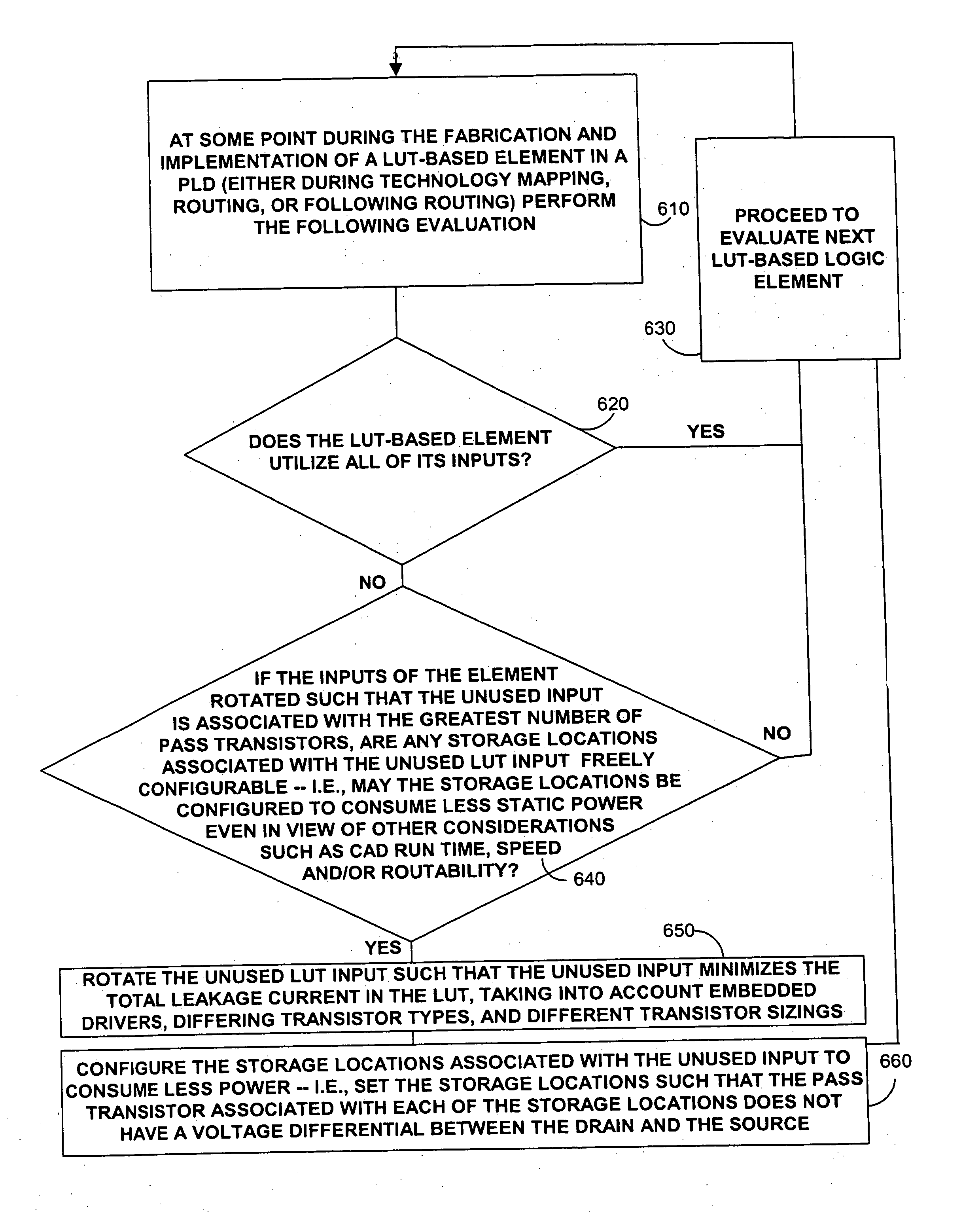
[0008] Systems and methods for reducing static and total power in a PLD according to the invention are provided. The systems and methods preferably reflect concepts that can be implemented to reduce leakage current of FETs as well as other power-saving concepts in a PLD. It should be noted that the effect of implementing these concepts should preferably be weighed against the deleterious effects of the implementation of these concepts on other PLD areas of importance—e.g., routability, Computer-Aided Design (CAD) run time, and speed of the circuitry implemented on the PLD.

Problems solved by technology

It follows that the source of power consumption in the static state of such a PLD having thin gate thicknesses tends to come from the leakage of the transistors in the PLD due to their passing current between VCC and GND, even when they are in the OFF position.
The majority of power consumption in the static state of a PLD which implements 90 nanometer line widths comes from leakage of FETs.
The leakage of the FETs results from a voltage differential existing between the drain and the source combined with the transistor not fully turning itself OFF.

Method used


Image

  • Systems and methods for reducing static and total power consumption in a programmable logic device
  • Systems and methods for reducing static and total power consumption in a programmable logic device
  • Systems and methods for reducing static and total power consumption in a programmable logic device

Examples


Embodiment Construction

[0013] It is common in programmable logic devices to provide logic elements which are based on look-up tables. For example, programmable logic devices available from Altera Corporation, of San Jose, Calif., may include logic elements built at least in part around four-input, or some other suitable number of inputs, look-up tables. The logic elements can be programmed and programmably interconnected to simulate any logic function.

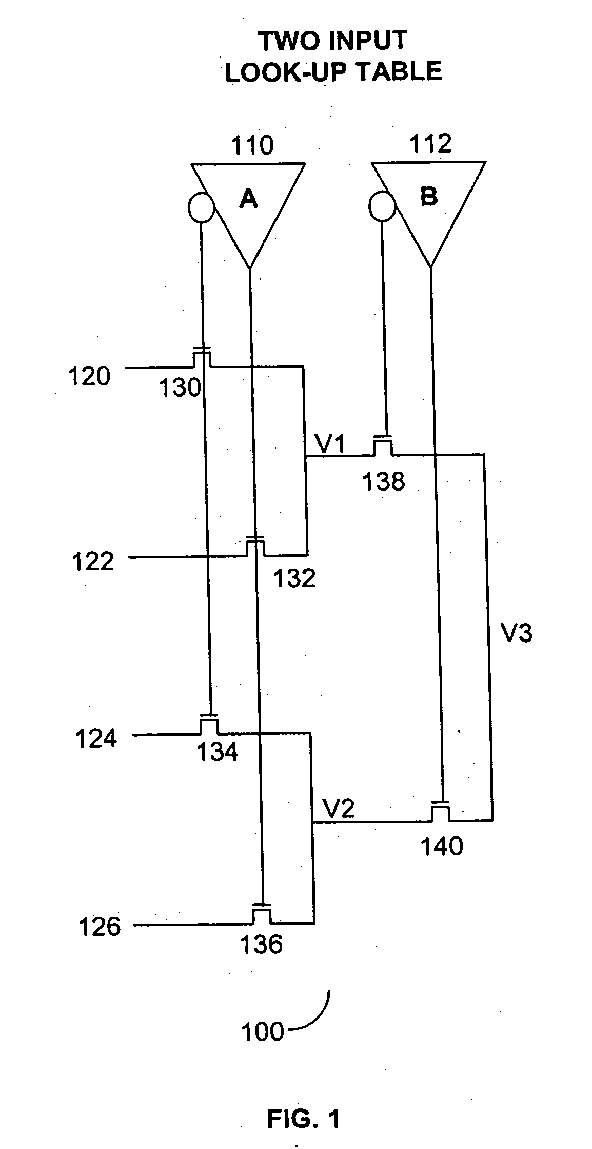
[0014]FIG. 1 shows a two-input look-up table (LUT) 100 that may be used in systems and methods according to the invention. LUT 100 preferably includes inputs 110 and 112 (which are also labeled as A and B in order to clarify examples described below in the application), storage locations 120, 122, 124, and 126 and pass transistors 130, 132, 134, 136, 138, and 140.

[0015] LUT 100 preferably operates as follows. The inputs receive a two-bit signal—i.e., 00, 01, 10, or 11. Then, in response to the two bit signal received at the input, the output of the LUT at ...


PUM


Abstract

A method and system for reducing power consumption in a programmable logic device (PLD) is provided. The power consumption may be reduced by preferably continually considering power consumption as a factor in circuit design during the technology mapping, routing, and period following routing of the programmable logic device.

Description

STATEMENT OF RELATED CASE [0001] This application is being filed together with co-pending U.S. patent application Ser. No. 10 / 796,502, entitled, “Systems and Methods for Reducing Static and Total Power Consumption in Programmable Logic Device Architectures”, which is hereby incorporated by reference herein in its entirety.BACKGROUND OF THE INVENTION [0002] This invention relates to reducing static and total power in electronic devices. More particularly, this invention relates to reducing static and total power consumption in a programmable logic device (PLD). [0003] Gate thickness of transistors in PLDs have always trended thinner and thinner. As the gate thicknesses approach 90 nanometers, the transistors do not fully turn OFF. Thus, a pass gate in the OFF position continues to pass some current. It follows that the source of power consumption in the static state of such a PLD having thin gate thicknesses tends to come from the leakage of the transistors in the PLD due to their pa...

Claims


Application Information

Patent Timeline
Patent Type & Authority Applications(United States)
IPC IPC(8): G06F1/00
CPCG06F1/32
Inventor MENDEL, DAVIDBETZ, VAUGHN
Owner ALTERA CORP
Learn More