

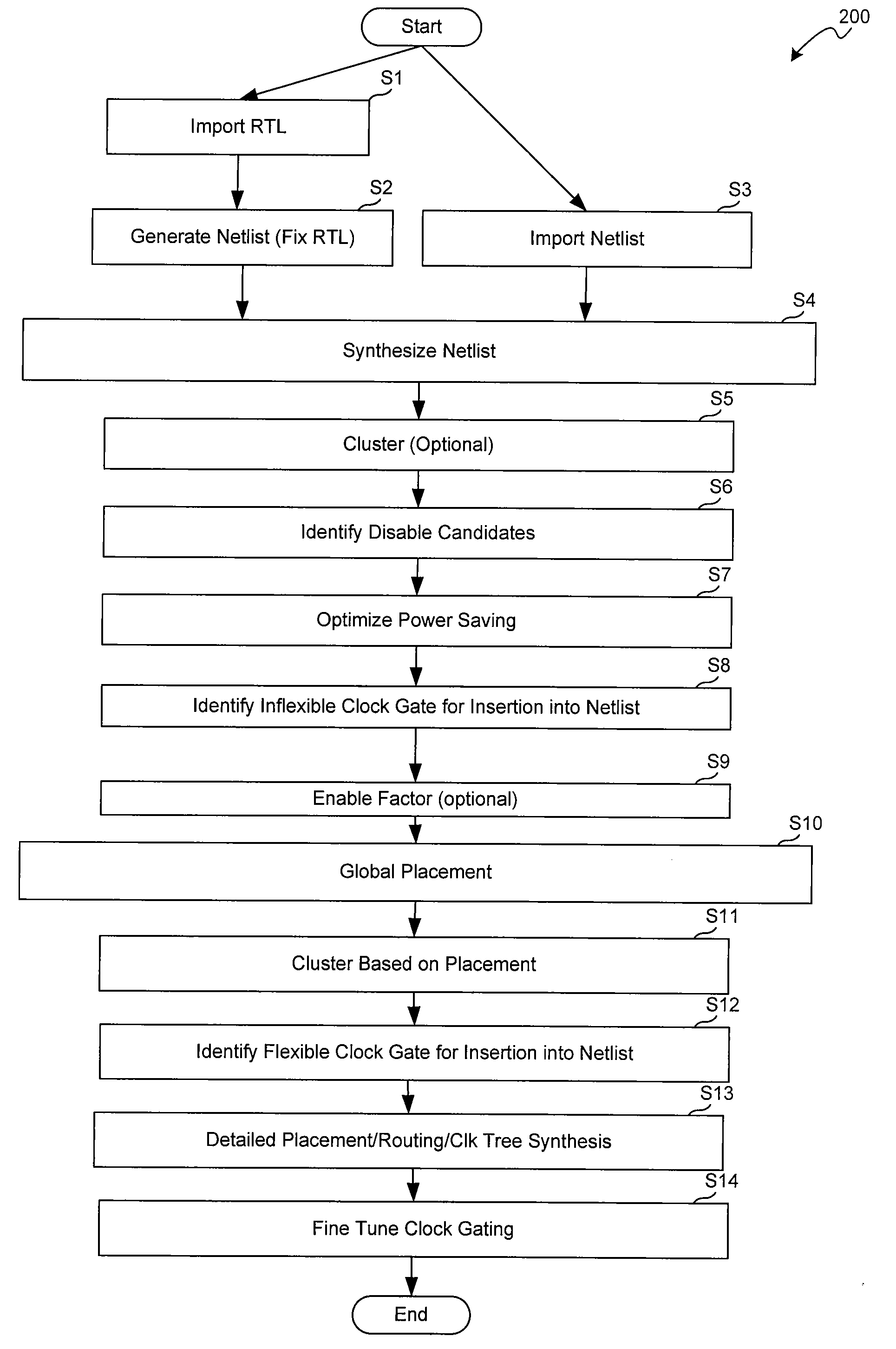
Method For Optimized Automatic Clock Gating
a technology of automatic clock gating and clock gating, which is applied in the direction of pulse manipulation, pulse technique, instruments, etc., can solve the problems of large amount of standby or static current, increased static power consumption with each new technology, and corresponding lower performance, so as to reduce the switching power consumed and consume less power
- Summary
- Abstract
- Description
- Claims
- Application Information
AI Technical Summary
Benefits of technology
Problems solved by technology
Method used
Image

Examples
Embodiment Construction
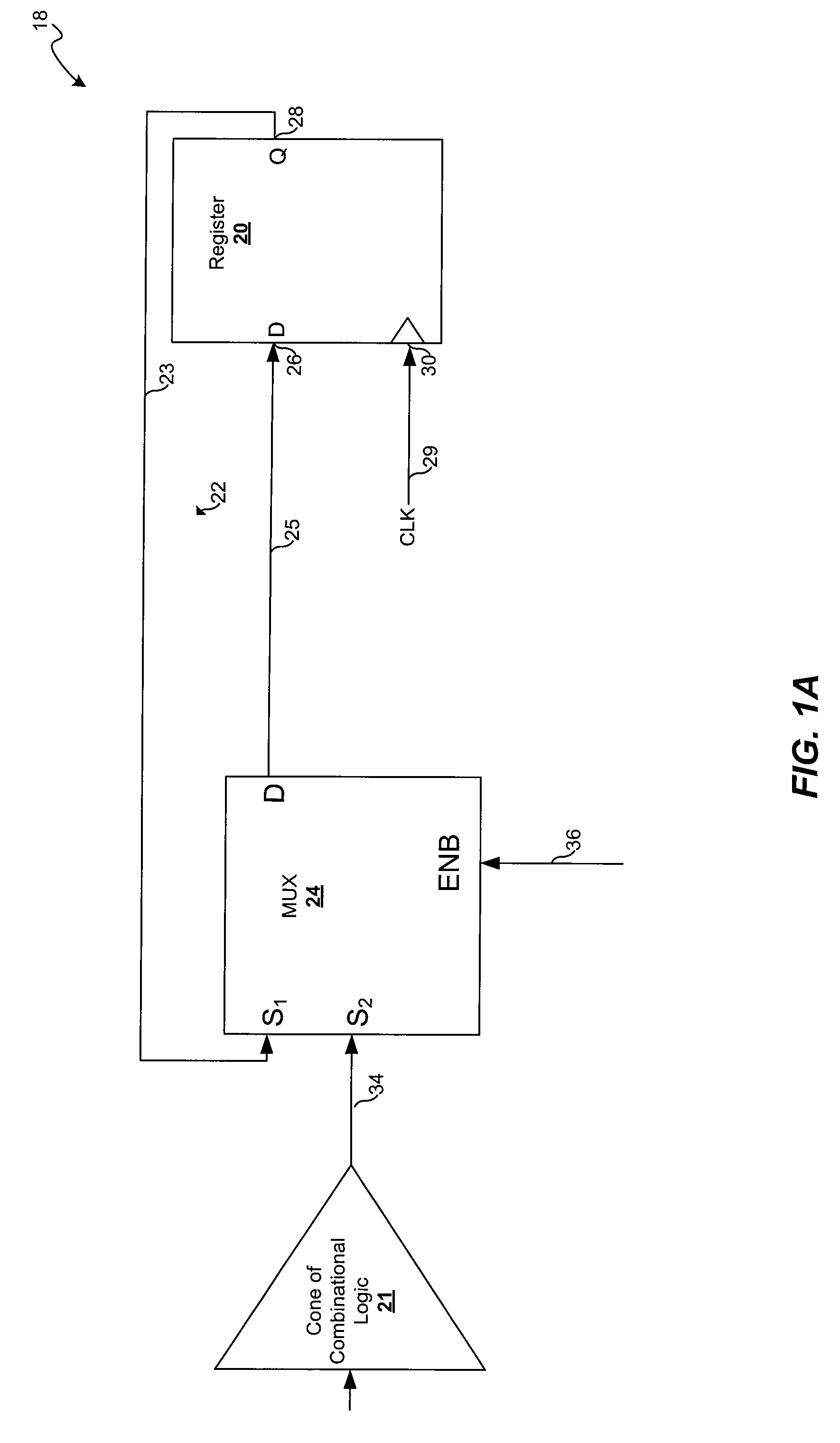
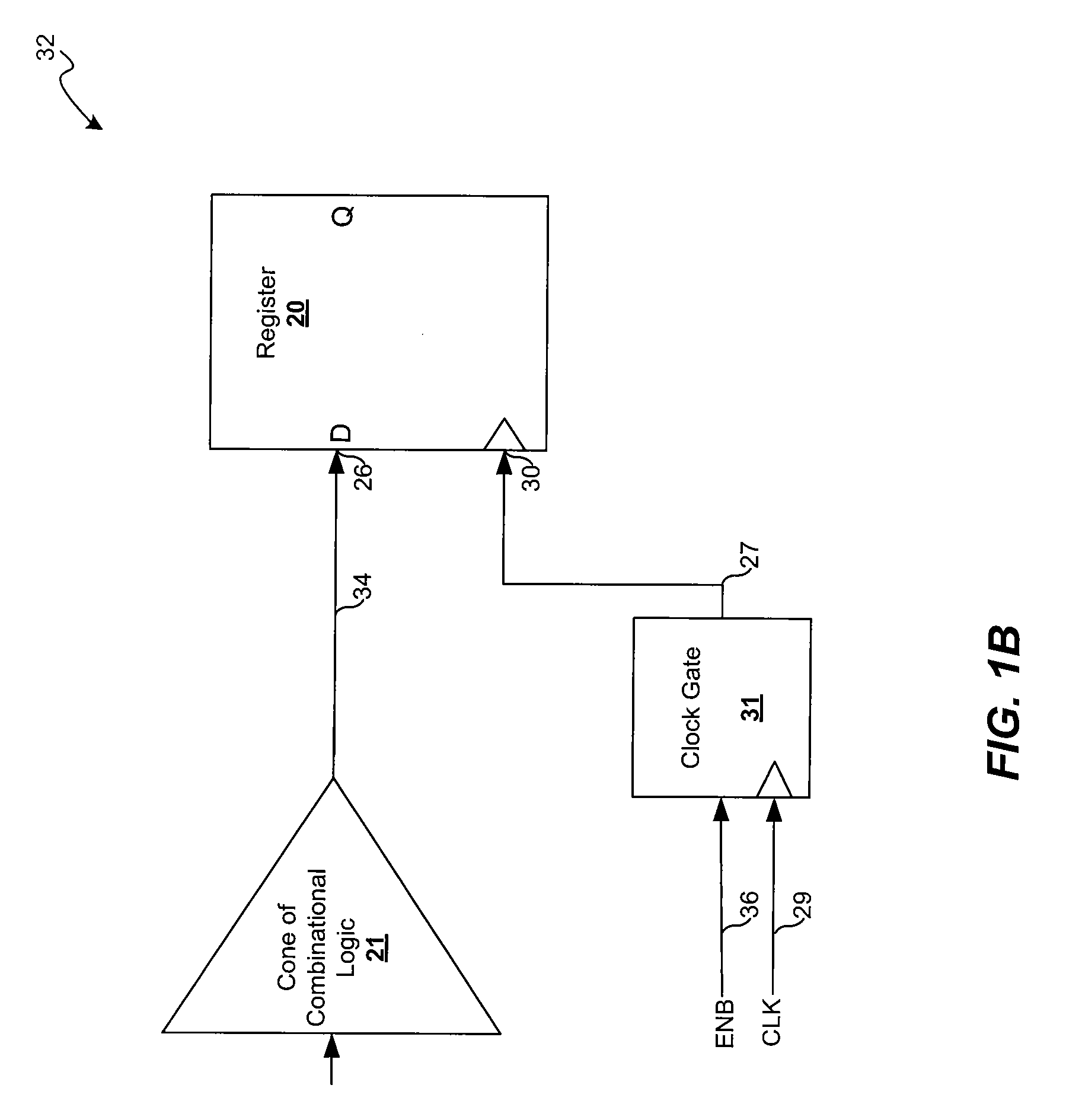
[0032]Although clock gating saves on-chip power, clock gating circuitry itself consumes power. Clock gating can be performed on a single storage element, commonly referred to as a flip flop (or even more simply as a flop), but the clock gating circuit area may be non-trivial. In one embodiment, simultaneously gating more than a single element at a time is performed. Traditionally, power consumption in integrated circuits has been reduced by clock-gating. This technique reduces the consumption of switching power. FIG. 1A is a schematic illustration of a pre-clock gated circuit design 18 which includes a sequential element associated with a feedback loop that includes arbitrary combinational logic circuitry. As shown, a sequential element 20 (i.e., register) is associated with a feedback loop 22 and arbitrary combinational logic circuitry 24. The combinational logic is shown conceptually as a multiplexer which includes input pins S1 and S2 and an enable ENB input. A cone of combinatio...
PUM
 Abstract
Description
Claims
Application Information