Negative voltage level switching circuit

A level switching, negative voltage technology, applied in the direction of logic circuit connection/interface layout, logic circuit coupling/interface using field effect transistors, etc., can solve the problem of increased circuit layout area, increased switching power consumption, and reduced switching speed etc. to achieve the effects of speeding up voltage switching, reducing switching power consumption, and improving circuit performance

Active Publication Date: 2011-11-30
GIGADEVICE SEMICON (BEIJING) INC
View PDF1 Cites 0 Cited by
  • Summary
  • Abstract
  • Description
  • Claims
  • Application Information

AI Technical Summary

Problems solved by technology

In order to ensure the switching is completed, the switching current of the P-channel transistor must also increase, but according to (1), the (V GS -V th ) absolute value is Vdd-V th is a constant value, in order to increase the saturation current, it must be increased However, the length L is generally determined by the process conditions of the CMOS process and cannot be reduced casually. That is, to increase this ratio, the width W must be increased.
According to the principle of integrated circuit manufacturing, since the main carrier of the P channel is holes, in order to obtain the same conductivity as the N channel transistor with electrons as the main carrier, the area of ​​the P channel transistor needs to be smaller than that of the N channel transistor. The channel transistor is several times larger, so increasing the width W of the P-channel transistor will lead to a significant increase in the circuit layout area
[0013] Second, according to the above analysis, with the decrease of Vneg, the switching current will increase, and obviously the switching power consumption will also increase
For the current process, under the condition of 0.18μm or smaller size, the switching power consumption already occupies a considerable proportion of the total power consumption of the circuit. Therefore, the increase of switching power consumption will have a great impact on the overall circuit
[0014] Third, the circuit is unstable, and the switching speed of the circuit is affected by Vdd. During the operation of the circuit, if Vneg decreases or Vdd decreases, the switching speed will decrease, and if the two decrease beyond a certain level, the P-channel The saturated conduction current of the transistor is less than that of the N-channel transistor, that is, the P-channel transistor cannot provide sufficient current conduction capability, and the circuit will enter a metastable state, and the voltage cannot be switched, causing a large DC power consumption
However, since the source of the P-channel transistor is not directly connected to VDD, but is connected to the input signal Vin or the reverse signal input signal Vin_b, although this circuit can make the entire negative high-voltage level conversion circuit reduce the input voltage At this time, the circuit can still work normally, but for such a structure, when the P-channel transistor uses the same area, the pull-up current reaches 1 / 4 of the previous circuit, that is, if the same pull-up current is to be achieved, P The channel transistor area will increase by 4 times. At the same time, increasing the P-channel transistor will also significantly increase the layout area of ​​the circuit.
Therefore, there are still many deficiencies in this circuit

Method used


Image

  • Negative voltage level switching circuit
  • Negative voltage level switching circuit
  • Negative voltage level switching circuit

Examples


Embodiment Construction

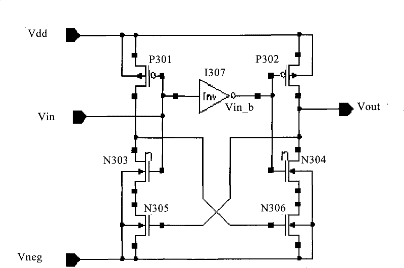
[0026] Negative voltage level switching circuit of the present invention such as image 3 shown. It includes an inverter I307, two P-channel metal oxide semiconductor field effect transistors (MOSFET) P301, P302; 4 N channel metal oxide semiconductor field effect transistors (MOSFET) N303, N304, N305, N306; for For the convenience of description, MOSFET will be referred to as transistor for short, P-channel metal oxide semiconductor field effect transistor (MOSFET) will be referred to as P channel transistor, and N channel metal oxide semiconductor field effect transistor (MOSFET) will be referred to as N channel transistor for short. .

[0027] see image 3 , wherein Vdd is a positive voltage, Vneg is a negative voltage, Vin is an input signal, the input signal of Vin is reversed after passing through the inverter I307, and the reverse input signal is Vin_b, and the output of the negative voltage level switching circuit is Vout. There are two sets of transistor circuits be...


PUM


Abstract

A negative voltage level switching circuit, including: 2 inserted N tubes; 2 pull-up P tubes, the sources of which are connected to the forward voltage Vdd, and the drains are respectively connected to the drains of the inserted N tubes; 2 positive feedback The source of the N tube is connected to the negative voltage Vneg, and the drains are respectively connected to the sources of the two inserted N tubes; the node between the second inserted N tube and the second pull-up P tube is the output Vout, and the first inserted The gates of the N tube and the first pull-up P tube are connected to the input signal Vin, the gate of the first positive feedback N tube is connected to the output voltage Vout; the second insertion N tube and the second pull-up P tube gate are connected to The output end of the inverter and the input end of the inverter are connected to the input signal Vin; the gate of the second positive feedback N transistor is connected to the node between the first insertion N transistor and the drain of the first pull-up P transistor. The conduction current required by the P tube can be reduced under the same conduction condition, and the area of ​​the P tube can be reduced; and the voltage switching speed can be accelerated and the switching power consumption can be reduced.

Description

technical field [0001] The present invention relates to integrated circuit design, in particular to a negative voltage switching circuit for switching an output voltage between a positive voltage and a negative voltage according to a transformation of an input signal. Background technique [0002] During the operation of an integrated circuit, different voltages are often required in order to adapt to various operations. The input voltage of a circuit is usually single or limited. Therefore, a circuit that can convert the input voltage into a positive high voltage or a negative high voltage required for different operations is required in the circuit design. [0003] Taking flash memory (Flash Memory) as an example, in the storage structure of a typical NOR-type Flash memory chip, each memory cell includes a MOSFET, whose gate is connected to the corresponding word line WL, and the drain is connected to the corresponding bit line BL , while the sources of all memory cells a...

Claims


Application Information

Patent Timeline
Patent Type & Authority Patents(China)
IPC IPC(8): H03K19/0185
Inventor 胡洪
Owner GIGADEVICE SEMICON (BEIJING) INC
Why Eureka
Try Eureka