

Buffer in ultra-low power consumption integrated circuit
An integrated circuit, ultra-low power consumption technology, applied in the buffer field, can solve the problem of large punch-through current, and achieve the effect of avoiding conduction current
- Summary
- Abstract
- Description
- Claims
- Application Information
AI Technical Summary
Problems solved by technology
Method used
Image

Examples
Embodiment Construction
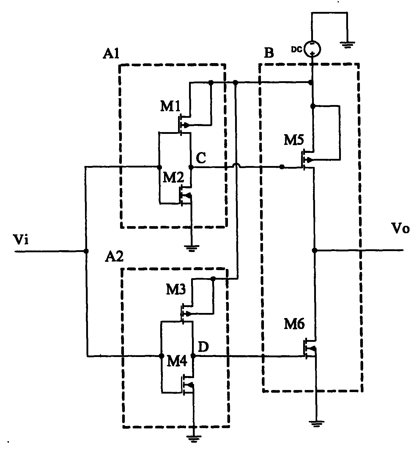
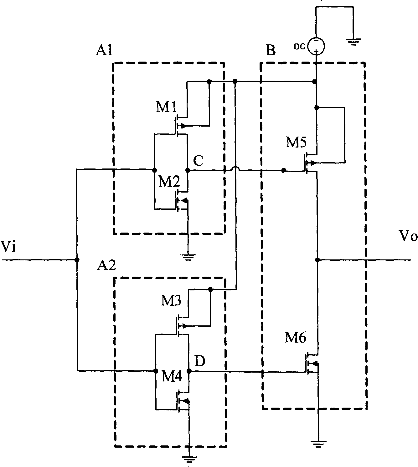
[0018] The present invention will be further described below with reference to FIG. 2. In FIG. 2, two first-stage inverters A1 and A2 are included. Among them, the first-stage inverter A1 includes a PMOS tube M1 and an NMOS tube M2 connected in series, and a PMOS tube The gate of M1 is connected to the gate of the NMOS tube M2 and connected to the voltage input terminal Vi. The gate of the PMOS tube M1 and the gate of the NMOS tube M2 are connected and converged at point C and used as the first-stage inverter A1 At the output end, the source of the PMOS tube M1 is connected to the power supply voltage, and the source of the NMOS tube M2 is grounded. The first-stage inverter A2 includes a PMOS tube M3 and an NMOS tube M4 connected in series. The gate of the PMOS tube M3 is connected to the gate of the NMOS tube M4 and connected to the voltage input terminal Vi. The gate of the PMOS tube M3 is connected to the NMOS tube. The gate of M4 converges at point D and serves as the outpu...
PUM
 Abstract
Description
Claims
Application Information