

Formation method of semiconductor structure
A semiconductor and gate structure technology, applied in the field of semiconductor structure formation, can solve the problems of FinFET performance to be improved, and achieve the effects of improving carrier mobility, preventing stress release, and improving performance
- Summary
- Abstract
- Description
- Claims
- Application Information
AI Technical Summary
Problems solved by technology
Method used
Image

Examples
Embodiment Construction
[0029] It can be known from the background art that the performance of FinFETs still needs to be improved at present.
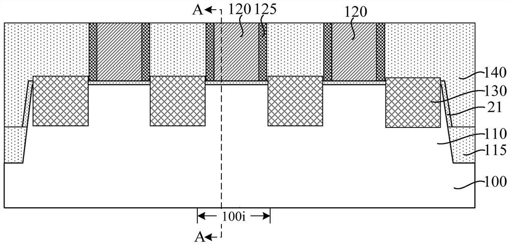
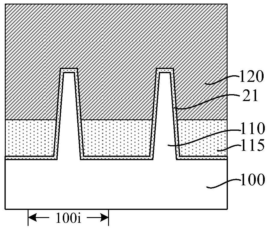
[0030] According to the analysis, taking PMOS as an example, in FinFET, the material of the fin is SiGe, which can provide compressive stress to the channel of the PMOS device, thereby improving the mobility of carriers.
[0031] In the process of forming the semiconductor structure, a fin cut process is usually performed, and after the fin part is formed, the fin part at the unneeded position is cut and removed in the fin cut process. However, performing the fin cutting process is likely to cause stress relief in the fins, which in turn leads to a poor effect of improving carrier mobility.
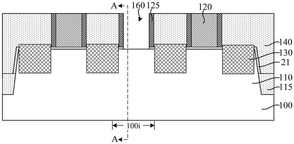
[0032] One method is to cut and remove the fins at unneeded positions after forming the dummy gate structure, the source and drain doped regions in the fins on both sides of the dummy gate structure, and the interlayer dielectric layer.
[0033] Although this approach c...
PUM
 Abstract
Description
Claims
Application Information