

Semiconductor structure and manufacturing method thereof
A semiconductor and isolation structure technology, applied in the field of semiconductor structure and its manufacturing, can solve the problems of scaling down, area reduction, increasing process steps, etc., to achieve the effect of improving integration, avoiding stress release, and improving utilization rate
- Summary
- Abstract
- Description
- Claims
- Application Information
AI Technical Summary
Problems solved by technology
Method used
Image

Examples
Embodiment Construction
[0025] The features and technical effects of the technical solution of the present invention will be described in detail below with reference to the accompanying drawings and in combination with exemplary embodiments. It should be pointed out that similar reference numerals represent similar structures, and the terms "first", "second", "upper", "lower" and the like used in this application can be used to modify various device structures. These modifications do not imply a spatial, sequential or hierarchical relationship of the modified device structures unless specifically stated.
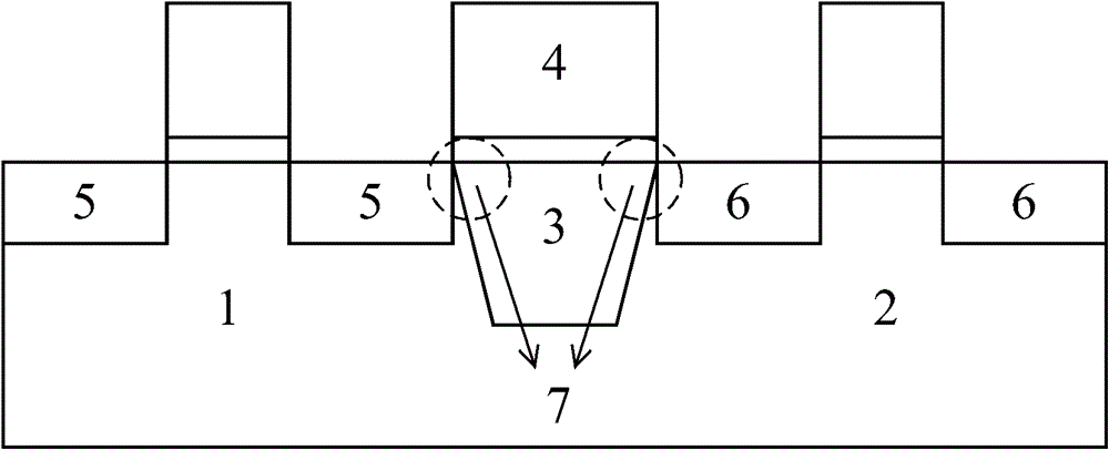
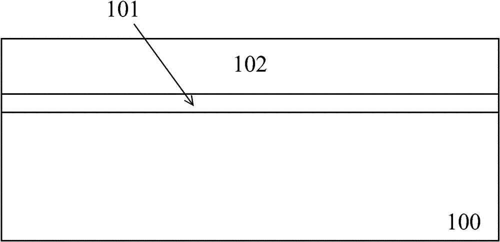
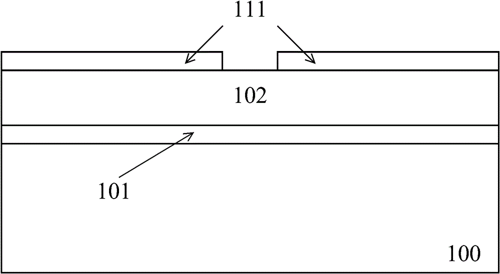
[0026] Such as Figure 7 Shown is a schematic diagram of an isolation structure of a semiconductor substrate obtained according to an embodiment of the present invention. The isolation structure, formed on the semiconductor substrate 100, includes: an isolation trench 104 embedded in the semiconductor substrate 100; a dielectric layer 105 filled in the isolation trench 104; wherein, the isolation ...
PUM
 Abstract
Description
Claims
Application Information