A kind of preparation method of gallium nitride-based light-emitting diode epitaxial wafer

A light-emitting diode, gallium nitride-based technology, applied in the direction of electrical components, circuits, semiconductor devices, etc., can solve the problems of poor antistatic ability of the chip, uneven thickness, uniformity of the epitaxial layer, etc., and achieve the effect of solving current congestion

Active Publication Date: 2017-12-29
TIANJIN SANAN OPTOELECTRONICS
View PDF5 Cites 0 Cited by
  • Summary
  • Abstract
  • Description
  • Claims
  • Application Information

AI Technical Summary

Problems solved by technology

[0003] In the conventional GaN-based diode epitaxial wafer structure, Al x Ga 1~x The N layer as an electron blocking layer or a stress releasing layer is made of N-type Al x Ga 1~x N monolayer or P-type Al x Ga 1~x N single-layer form exists. With the development of technology, this structure is far from meeting the requirements of high-power LED chips, resulting in poor antistatic ability of the chip, uneven current distribution and uneven light-emitting area, especially in the growth of large-scale epitaxial wafers. In the process, the uniformity of the epitaxial layer is greatly affected, so that the Al x Ga 1~x N single-layer thickness is uneven, resulting in poor uniformity of light emission and low average brightness

Method used


Image

  • A kind of preparation method of gallium nitride-based light-emitting diode epitaxial wafer
  • A kind of preparation method of gallium nitride-based light-emitting diode epitaxial wafer
  • A kind of preparation method of gallium nitride-based light-emitting diode epitaxial wafer

Examples


Embodiment 1

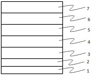
[0035] Figure 1~6 This is a schematic diagram of manufacturing a gallium nitride-based light-emitting diode epitaxial wafer according to the present invention. The epitaxial wafer prepared in this embodiment includes from bottom to top: (1) sapphire substrate 1; (2) low temperature nitride buffer layer 2, Can contain gallium nitride, or aluminum nitride or a combination of both, the film thickness is between 10-100nm; (3) the gallium nitride substrate layer 3, the film thickness is between 300-7000nm, preferably 3500nm; (4)N Type gallium nitride layer 4, where the doping source is silane, and the doping concentration is 1×10 18 ~2×10 19 cm -3 Between, preferably 1.2×10 19 cm -3 ; (5) Multiple quantum well active region 5, with In y Ga 1-y N as well layer, gallium nitride or Al x Ga 1~x N or a combination of the two are used as a barrier layer, where the thickness of the barrier layer is between 50 and 150 nm, and the thickness of the well layer is between 1 and 20 nm; (6) The l...

Embodiment 2

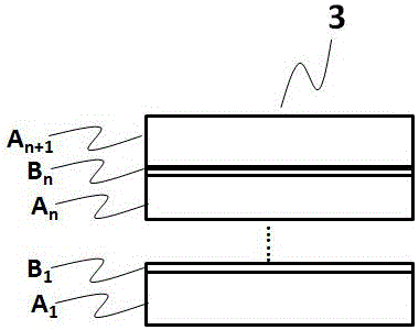
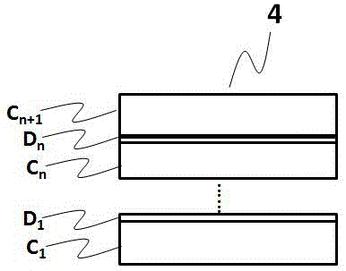
[0045] Such as Figure 7 As shown, different from Embodiment 1, in this embodiment, during the growth process of the gallium nitride substrate layer, the N-type gallium nitride layer, the low-temperature P-type layer, and the high-temperature P-type layer, only the gallium source ( Or including an indium source), the ammonia gas remains in the state of passing, so that Al is formed in the GaN substrate layer, N-type GaN layer, low-temperature P-type layer, and high-temperature P-type layer x Ga 1~x The aluminum component x value of the N layer presents a structure that first increases from 0 to 1 and then decreases to 0. This structure makes B n , D n , F n , H n The aluminum component in the GaN is greatly increased, thus strengthening the stress relief effect in the gallium nitride substrate layer, and forming a higher barrier in the N-type gallium nitride layer and the high-temperature P-type layer, strengthening the current expansion, The electron blocking effect in the low-t...


PUM

PropertyMeasurementUnit
thicknessaaaaaaaaaa
thicknessaaaaaaaaaa
thicknessaaaaaaaaaa

Abstract

The invention provides a preparation method of a gallium nitride-based light emitting diode epitaxial wafer. The preparation method comprises the following steps: (1) carrying out heat treatment on a substrate; (2) sequentially growing a low-temperature buffer layer, a gallium nitride-based plate layer, an N-type gallium nitride layer, a multi-quantum-well active region, a low-temperature P-type layer and a high-temperature P-type layer on the substrate after the heat treatment; (3) growing AlxGa1-xN layers by utilizing manners of closing a gallium source and introducing an aluminum source within a short time in the growing processes of the gallium nitride-based plate layer, the N-type gallium nitride layer, the low-temperature P-type layer and the high-temperature P-type layer. According to the preparation method, the stress accumulated in a growth process of the epitaxial wafer can be effectively released by controlling the introducing frequency of the aluminum source, controlling whether to introduce ammonia gas as well as controlling the introducing quantity of the aluminum source; an electronic barrier layer is formed in the low-temperature P-type layer so as to barrier electrons from overshooting a P-type region; two-dimensional electron gas having a certain gradient distribution is generated in the N-type gallium nitride layer and the high-temperature P-type layer, so that the epitaxial performance is improved.

Description

Technical field [0001] The invention relates to the field of epitaxial gallium nitride semiconductor devices, in particular to a method for preparing an epitaxial wafer of a gallium nitride based light emitting diode. Background technique [0002] Light Emitting Diode (Light Emitting Diode in English, abbreviated as LED) is a semiconductor solid light-emitting device, which uses a semiconductor PN junction as a light-emitting structure, which can directly convert electricity into light. When a forward voltage is applied to both ends of the semiconductor PN junction Later, the minority carriers injected into the PN junction and the majority carriers recombine, and the excess energy is released to cause photon emission, which directly emits light of various colors. However, with the requirements for high-efficiency light-emitting chips, the key factors that need to be resolved include increasing the luminous intensity, improving the brightness uniformity, and improving the antistat...

Claims


Application Information

Patent Timeline
Patent Type & Authority Patents(China)
IPC IPC(8): H01L33/00H01L33/12H01L33/14
CPCH01L33/0066H01L33/0075H01L33/12H01L33/14
Inventor 舒立明张东炎刘晓峰王良钧王笃祥
Owner TIANJIN SANAN OPTOELECTRONICS
Why Eureka
Try Eureka