Method and apparatus for conversion between quasi differential signaling and true differential signaling

a technology of quasi-differential signaling and conversion method, applied in the field of digital signal active signal management, can solve the problems of electromagnetic interference, interconnection is a particular source of signal degradation, and the reliability and reach of transmitted digital signals are reduced,

Inactive Publication Date: 2007-05-10
XEMI
View PDF62 Cites 41 Cited by
  • Summary
  • Abstract
  • Description
  • Claims
  • Application Information

AI Technical Summary

Problems solved by technology

However, as device speeds increase, the analog effects exhibited by a digital signal due to device features can cause substantial distortion in the transmitted digital signal, thereby decreasing the reliability and reach of the transmitted digital signal.
Further, ring noise and the emission of electromagnetic interference (EMI) by the interconnect during the transmission of the signal can result in a degradation of the signal.
Interconnects are a particular source of signal degradation and electromagnetic interference (EMI) due to their particular physical and operational characteristics, such as relatively long signal transmission lengths, paired interconnect length mismatches, and lack of substantial shielding.
By disabling the functionality of the circuitry, however, the signal quality and EMI reduction benefits provided by the circuitry of the devices are diminished or eliminated.
Further, in the event that it is not feasible to disable the circuitry of a transmitting device or a receiving device, one or both of the devices may be inoperable with the other, thereby preventing their joint integration.
A device manufacturer or device provider therefore often is faced with a choice between utilizing circuitry at the device for improving signal quality thereby running the risk of rendering the device incompatible with other devices, or eliminating or severely limiting the use of any such circuitry, thereby increasing the likelihood of signal distortion and increased emitted EMI.

Method used


Image

  • Method and apparatus for conversion between quasi differential signaling and true differential signaling
  • Method and apparatus for conversion between quasi differential signaling and true differential signaling
  • Method and apparatus for conversion between quasi differential signaling and true differential signaling

Examples


Embodiment Construction

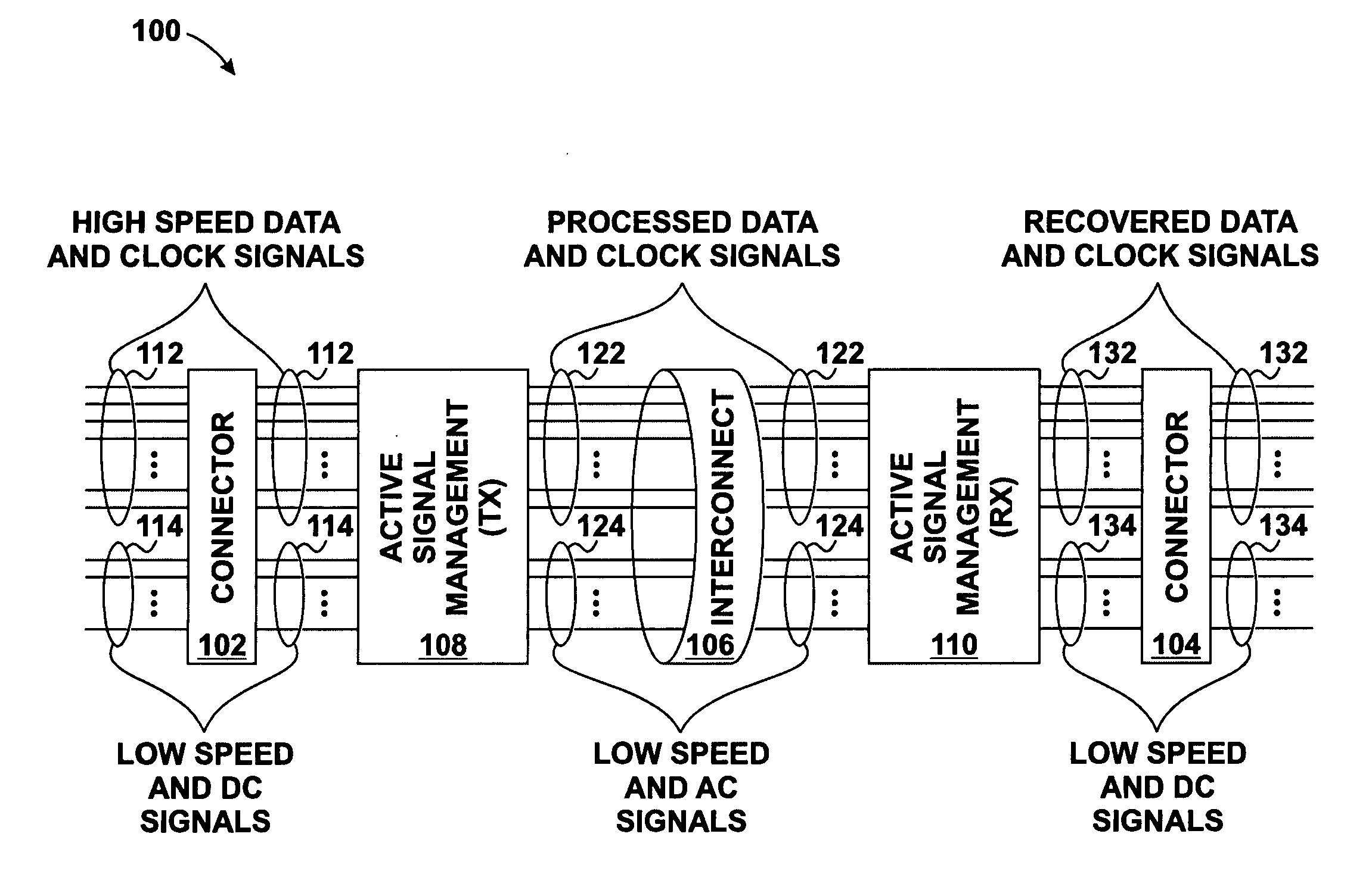
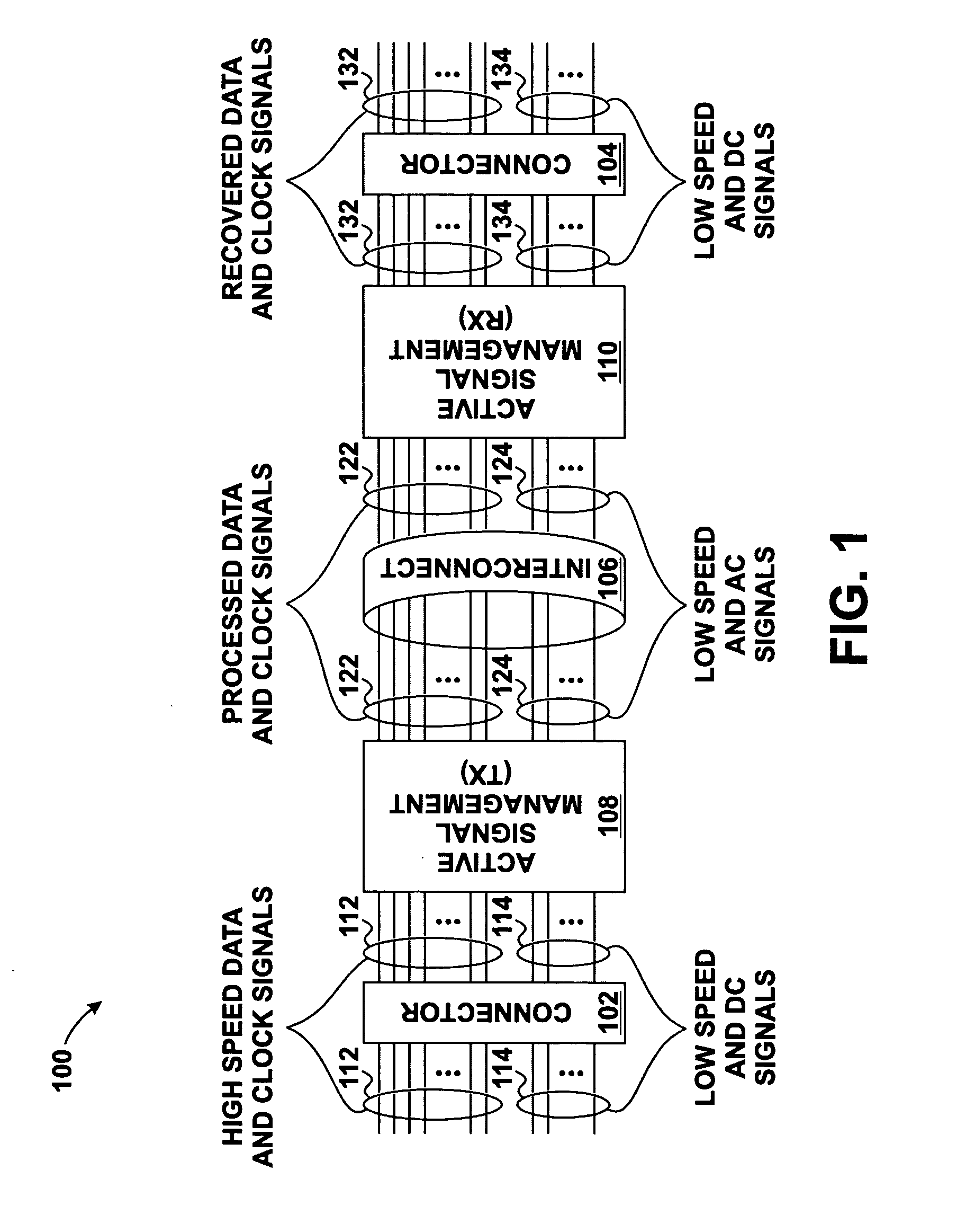
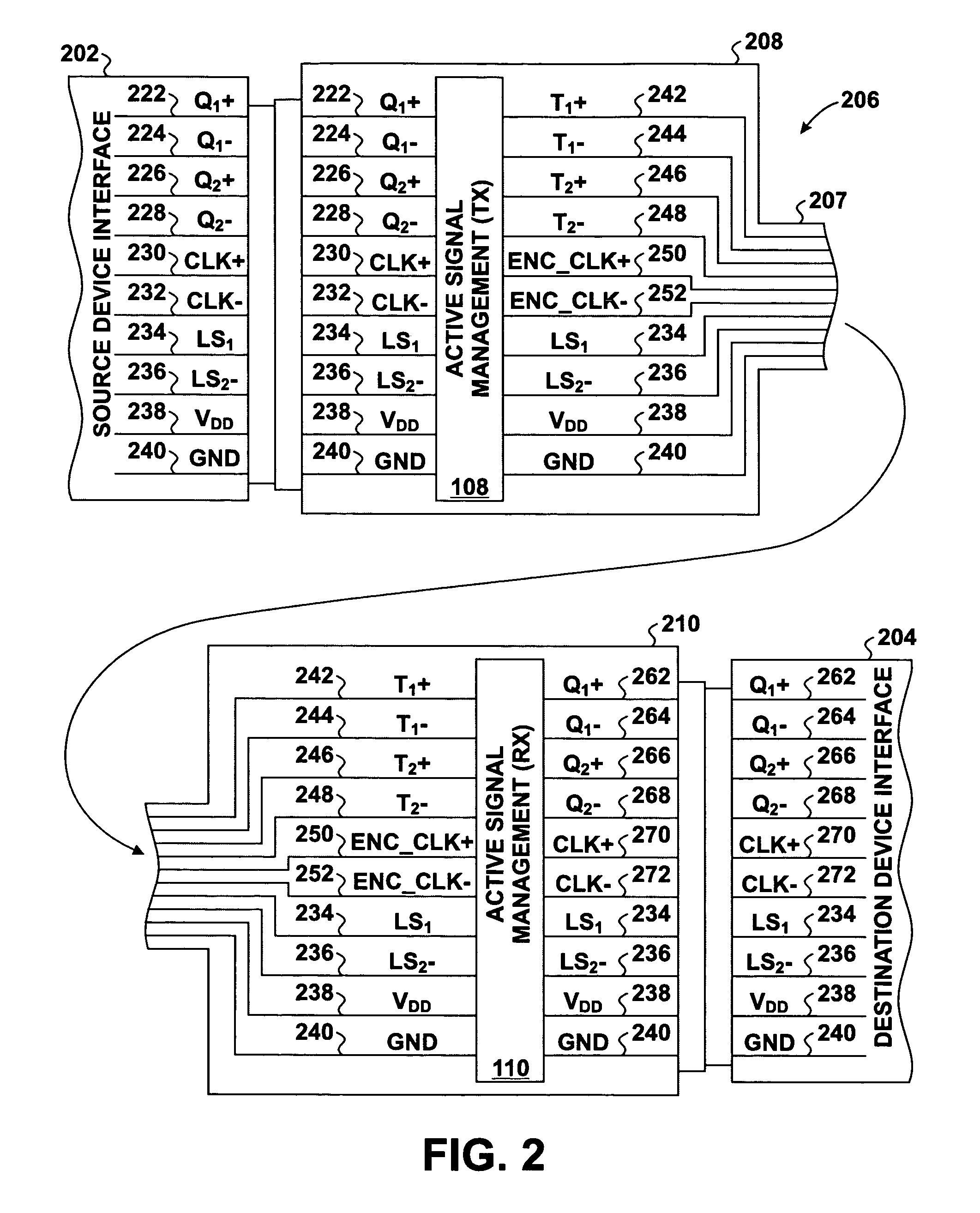
[0049]FIGS. 1-40 illustrate active signal management techniques for improving the quality or fidelity of a digital signal transmitted via an interconnect. In at least one embodiment, transmit-side active signal management circuitry applies one or more signal management processes to a digital signal at a transmit side of the interconnect. At the receive side of the interconnect, receive-side active signal management circuitry applies one or more corresponding active signal management processes, as appropriate, to the received digital signal to recover the information represented by the original digital signal. In one embodiment, the interconnect comprises a cable used to transmit the signals between a source device and a destination device, whereby one or both of the transmit-side active signal management circuitry and the receive-side active signal management circuitry is implemented at a corresponding cable receptacle of the cable. In another embodiment, one or both of the transmit...


PUM


Abstract

Transmit-side active signal management circuitry applies one or more active signal management processes to a digital signal at a transmit side of an interconnect. At the receive side of the interconnect, receive-side active signal management circuitry applies one or more corresponding active signal management processes, as appropriate, to the received digital signal to recover the information represented by the original digital signal. The interconnect can include a cable used to transmit the signals between a source device and a destination device, whereby one or both of the transmit-side active signal management circuitry and the receive-side active signal management circuitry is implemented at a corresponding cable receptacle of the cable. Alternately, one or both of the transmit-side active signal management circuitry and the receive-side active signal management circuitry can be implemented at a cable adaptor, thereby permitting the use of a passive cable interconnect to transmit the signal.

Description

CROSS-REFERENCE TO RELATED APPLICATIONS [0001] The present application claims priority to U.S. patent application Ser. No. 60 / 736,111 (Attorney Docket No. 1009-0009-P) filed Nov. 10, 2005 and entitled “System and Method of EMI Reduction in Digital Video Interfaces,” the entirety of which is incorporated by reference herein. The present application also claims priority to U.S. patent application Ser. No. 60 / 810,980 (Attorney Docket No. 1009-0009-P2) filed Jun. 6, 2006 and entitled “System and Method for Reduction of EMI in Cables and Other Interconnects,” the entirety of which is incorporated by reference herein. [0002] The present application is related to the following applications, the entireties of which are incorporated by reference herein: U.S. patent application Ser. No. ______(Attorney Docket No. 1009-0016), filed on even date herewith and entitled “Active Signal Management in Cables and Other Interconnects”; U.S. patent application Ser. No. ______(Attorney Docket No. 1009-00...

Claims


Application Information

Patent Timeline
Patent Type & Authority Applications(United States)
IPC IPC(8): H03K5/01
CPCG06F3/14G09G5/006G09G5/008G09G2330/06G09G2370/04G09G2370/10G09G2370/12H03K5/135H03K19/00346H03K19/00361H03K19/0175H03M9/00H04L25/14
Inventor EGAN, KENNETH W.SHEAFOR, STEPHEN J.CHANDLER, GREGORY T.BREHMER, GEOFFREY E.
Owner XEMI
Why Eureka
Try Eureka