Substrate with a spacer, panel, liquid crystal display panel, method of manufacturing panel and method of manufacturing liquid crystal display panel

Inactive Publication Date: 2007-05-31
SHARP KK
View PDF18 Cites 26 Cited by
  • Summary
  • Abstract
  • Description
  • Claims
  • Application Information

AI Technical Summary

Benefits of technology

[0041] The invention can provide the liquid crystal display panel that does not complicate the adhering operations, and prevent lowering of the display quality, and can also provide the method of manufacturing the same.
[0042] According to an aspect of the invention, uniform cell gaps can be obtained on the surfa

Problems solved by technology

This method of sealingly storing the liquid crystal in the vacuum filling method suffers from a problem that the filling time increases with the size of the liquid crystal display panel.
However, this manner suffers from a problem of occurrence of irregular display due to irregular dispersion or movement of the beads.
However, the liquid crystal material thermally extends in a high-temperature state so that the column-structure spacers cause irregular display due to nonuniformity in cell gap on the surface.
However, the spacer disclosed in the above patent reference has a high aspect ratio, and therefore is less resistant to elastic deformation so that the spacers

Method used


Image

  • Substrate with a spacer, panel, liquid crystal display panel, method of manufacturing panel and method of manufacturing liquid crystal display panel
  • Substrate with a spacer, panel, liquid crystal display panel, method of manufacturing panel and method of manufacturing liquid crystal display panel
  • Substrate with a spacer, panel, liquid crystal display panel, method of manufacturing panel and method of manufacturing liquid crystal display panel

Examples


first embodiment

[0075] Referring to FIGS. 1A-7B, description will now be given on a liquid crystal display panel and a method of manufacturing the same of a first embodiment of the invention.

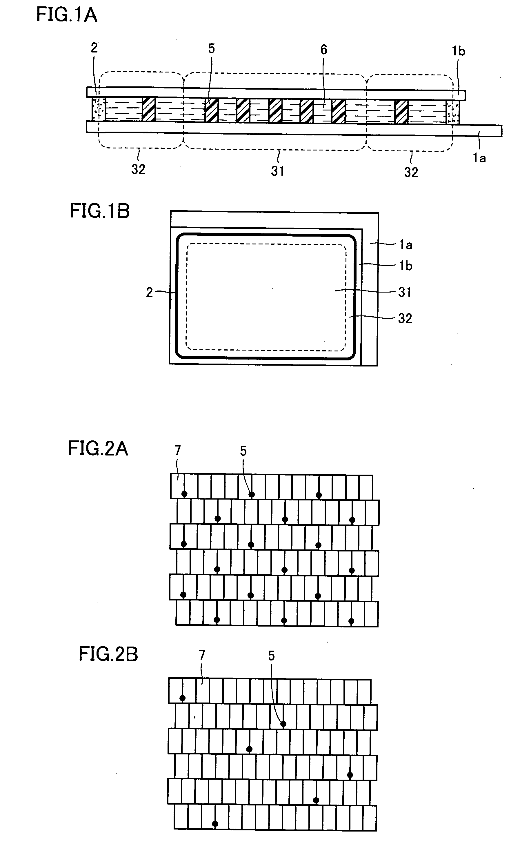
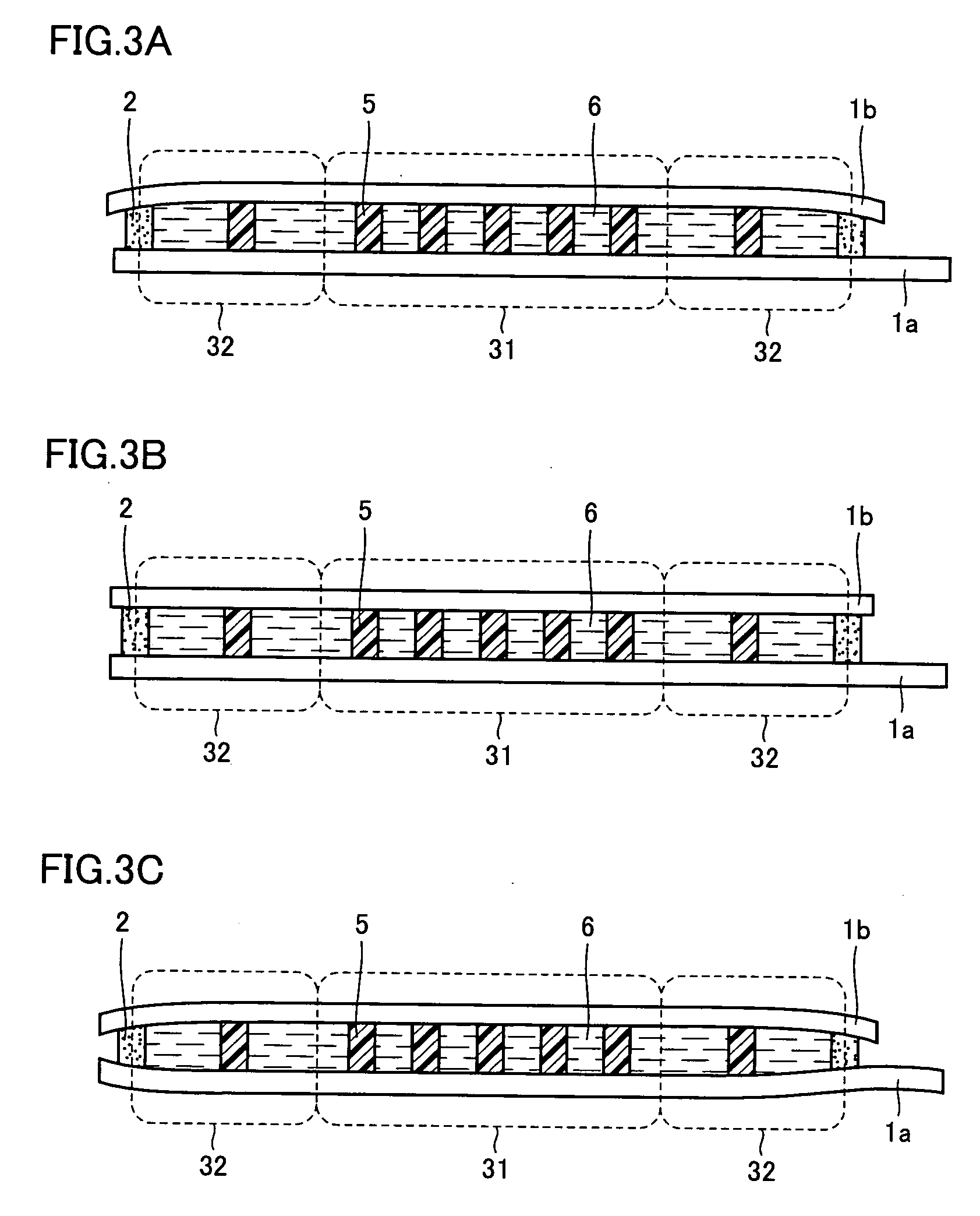
[0076]FIGS. 1A and 1B illustrate a first liquid crystal display panel of the embodiment. FIGS. 1A and 1B are a schematic cross section and a schematic plan, respectively. As shown in FIG. 1A, two substrates 1a and 1b are adhered and fixed together by a seal member 2. Substrate 1a is provided at its main surface with drive elements and others, and substrate 1b is provided at its main surface with opposed electrodes (not shown) and others. An inner space or region surrounded by two substrates 1a and 1b and seal member 2 is sealingly filled with liquid crystal 6. Substrates 1a and 1b are adhered and fixed together with a space therebetween. Columnar spacers 5 determine the distance between the two substrates.

[0077] Columnar spacers 5 are arranged in the region filled with the liquid crystal. Columnar spacer 5 ha...

second embodiment

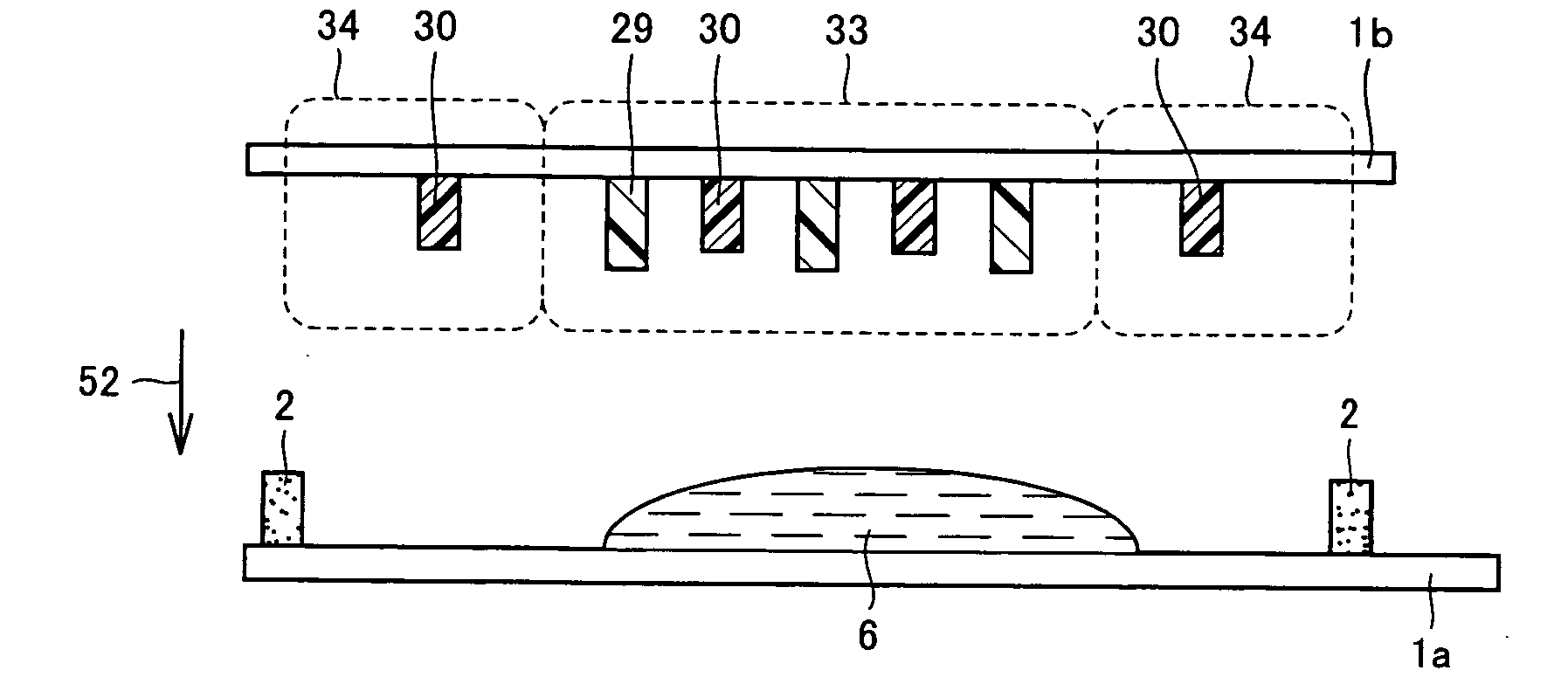
[0097] Referring to FIGS. 8A and 10, description will now be given on a liquid crystal display panel of a second embodiment according to the invention as well as a method of manufacturing the liquid crystal display panel.

[0098]FIGS. 8A and 8B illustrate the liquid crystal display panel of this embodiment. FIG. 8A is a schematic cross section, and FIG. 8B is a schematic plan. Two substrates 1a and 1b are fixed together by seal member 2, and the space surrounded by two substrates 1a and 1b and seal member 2 is filled with liquid crystal, as is done in the liquid crystal display panel of the first embodiment.

[0099] The liquid crystal display panel of this embodiment includes a low spacer arrangement region 34 as a first region near the inner side of seal member 2, and also includes a high-low spacer arrangement region 33 as a second region located inside low spacer arrangement region 34. The liquid crystal display panel includes first columnar spacers arranged in low spacer arrangeme...

third embodiment

[0116] This embodiment will now be described in connection with a substrate with spacers for use in a liquid crystal panel. The substrate with spacers according to the invention can be used not only in the liquid crystal panel but also in an organic EL panel, inorganic EL panel, plasma panel, field emission panel, electrochromic panel and others. The liquid crystal panel can be applied not only to the liquid crystal display panel but also to a picture shift panel that optically and successively shifts pixels as well as a parallax barrier panel that allows display of three-dimensional pictures. The picture shift panel includes at least one set of the liquid crystal panel modulating a polarization state of light and birefringent elements combined with the liquid crystal panel for shifting a light path according to the polarization state of light coming from the liquid crystal panel. The parallax barrier panel is combined with picture display elements having pixels for the left eye and...


PUM


Abstract

A liquid crystal display panel includes two substrates fixed together by a seal member with their main surfaces opposed to each other, liquid crystal sealingly stored in a region surrounded by the two substrates and the seal member, and a plurality of columnar spacers arranged in a region surrounded by the two substrates and the seal member. A number density of the columnar spacers in a low-density region near the inner side of the seal member is smaller than that in a high-density region inside the low-density region. The substrate with the spacer has the substrate and the spacer formed on the substrate. The spacer has at least a first spacer portion, and a second spacer portion formed above the first spacer portion. An upper portion of the first spacer has a larger diameter than a bottom of the second spacer portion.

Description

TECHNICAL FIELD [0001] The present invention relates to a liquid crystal display panel and a method of manufacturing the same, and particularly to a liquid crystal display panel including a columnar spacer as well as a method of manufacturing the same. [0002] Also, the present invention relates to a substrate provided with a spacer arranged on the substrate. The substrate with the spacer according to the invention is adhered to a substrate opposed thereto, and thereby a constant space can be kept between these substrates. BACKGROUND ART [0003] A liquid crystal display panel includes a substrate provided with drive elements for driving liquid crystal as well as a substrate provided with opposed electrodes opposed thereto, and these substrates are adhered together with their main surfaces opposed to each other with a space of several micrometers therebetween. [0004]FIG. 11 is a schematic cross section of a liquid crystal display panel according to a prior art. For the sake of simplici...

Claims


Application Information

Patent Timeline
IPC IPC(8): G02F1/1339G02F1/1333
CPCG02F2001/13396G02F1/13394G02F1/13396G02F1/1339G02F1/1341
Inventor YOKOYAMA, NAOTOUSUKURA, NARU
Owner SHARP KK
Why Eureka
Try Eureka