Method of manufacturing NAND flash memory device

a manufacturing method and flash memory technology, applied in the direction of semiconductor devices, electrical appliances, basic electric elements, etc., can solve the problems of etching and damage accordingly, so as to prevent the damage of the semiconductor substrate between the edge cell gate and the selection ga

Inactive Publication Date: 2007-05-31
SK HYNIX INC
View PDF1 Cites 3 Cited by
  • Summary
  • Abstract
  • Description
  • Claims
  • Application Information

AI Technical Summary

Benefits of technology

[0012] In one embodiment, the invention provides a method of manufacturing a NAND flash memory device, in which when forming spacers on sidewalls of selection gates, damage to a semiconductor substrate between edge cell gates and the selection gates can be prevented by selecting the distance between the edge cell gate and the selection gate, which is wider than the distance between center cell gates, but is narrower than the distance between the selection gates.
[0013] In another embodiment, the invention provides a method of manufacturing a NAND flash memory device, in which after forming an oxide film for forming spacers on sidewalls of a selection gate, a nitride film is formed on the oxide film between the edge cell gate and the selection gate, whereby a semiconductor substrate between the edge cell gate and the selection gate can be prevented from being damaged when the oxide film is etched in order to form the spacers.

Problems solved by technology

As a result, in the process of blanket-etching the nitride film to form the spacers on the sidewalls of the selection gate, the semiconductor substrate between the edge cell gate and the selection gate is etched and damaged accordingly.

Method used


Image

  • Method of manufacturing NAND flash memory device
  • Method of manufacturing NAND flash memory device
  • Method of manufacturing NAND flash memory device

Examples


Embodiment Construction

[0022] The invention will now be described in detail in connection with certain exemplary embodiments with reference to the accompanying drawings.

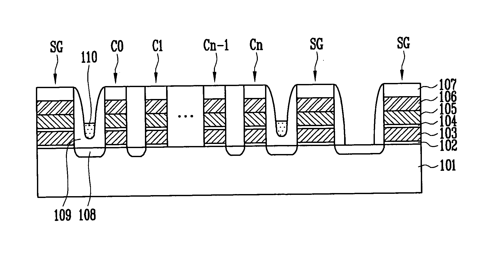
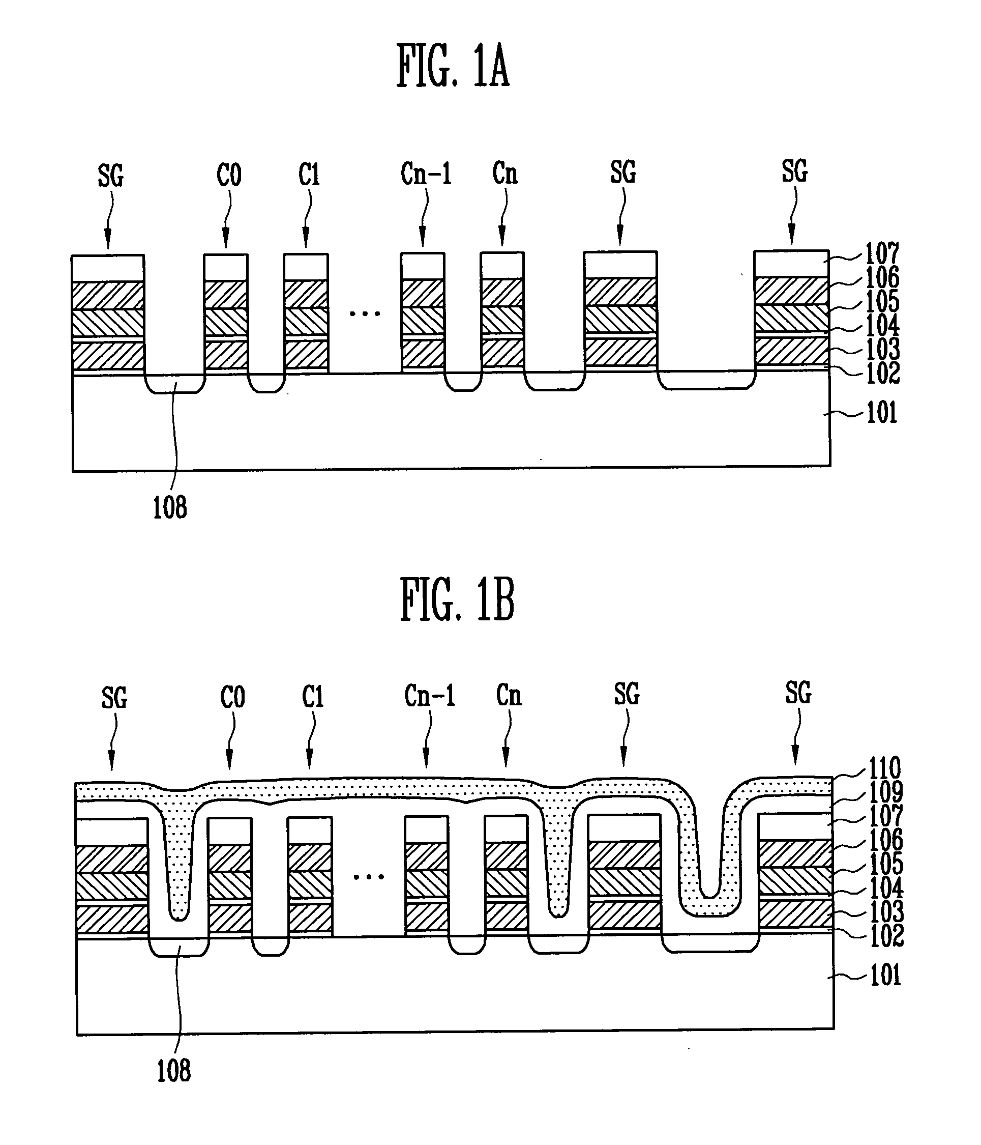
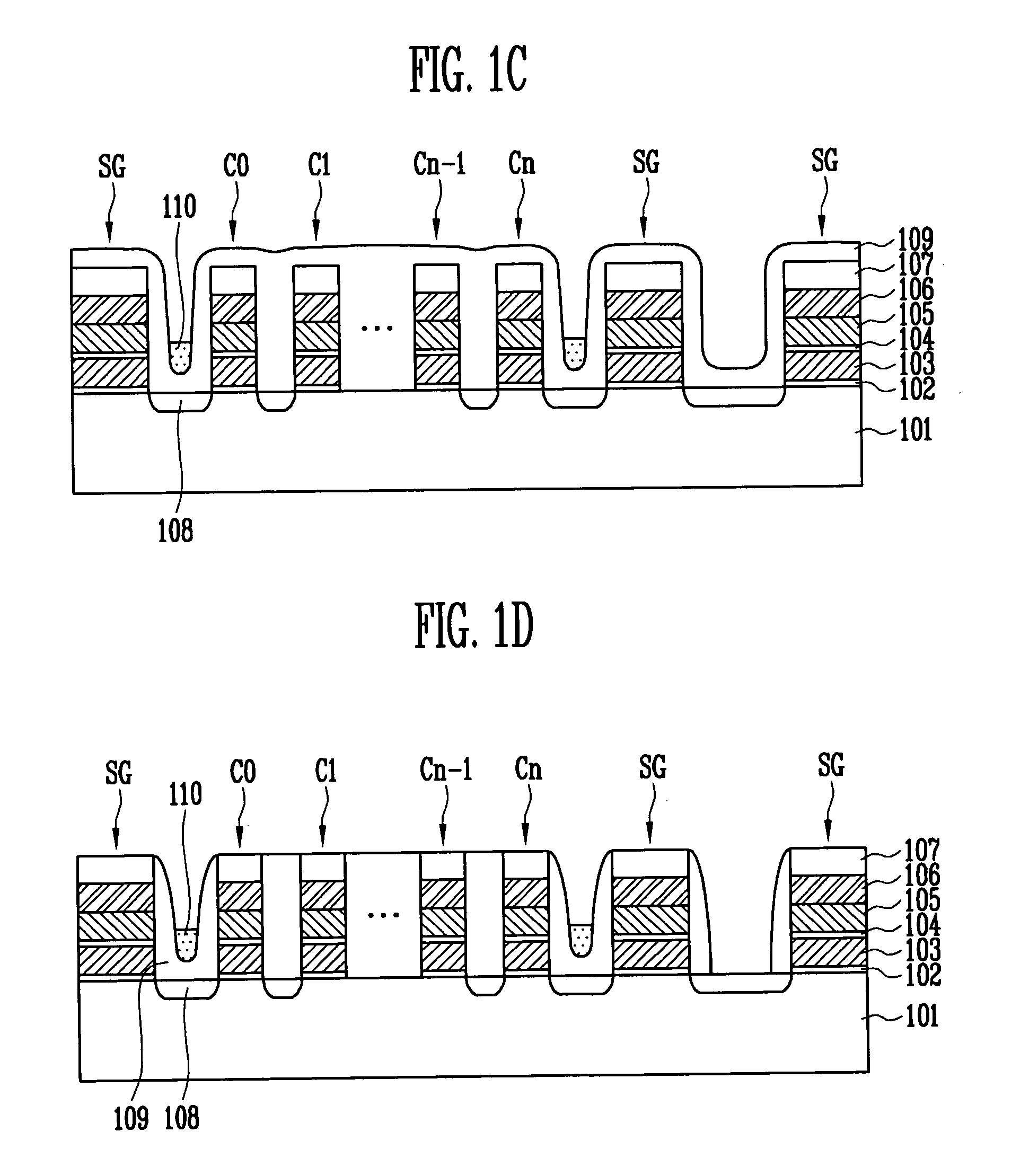
[0023]FIGS. 1A to 1D are cross-sectional views illustrating a method of manufacturing a NAND flash memory device according to an embodiment of the invention.

[0024] Referring to FIG. 1A, a tunnel oxide film 102, a first polysilicon layer 103, a dielectric layer 104, a second polysilicon layer 105, a tungsten film 106, and a hard mask film 107 are sequentially laminated on a region of a semiconductor substrate 101 in which a cell region, a select transistor region, and so on are defined through suitable processes, such as an isolation film formation process and a well formation process, for example. The dielectric layer 104 of the select transistor region is partially etched so that the first polysilicon layer 103 and the second polysilicon layer 105 are interconnected.

[0025] Accordingly, a plurality of cell gates C0, . . . , Cn in which ...


PUM


Abstract

A method of manufacturing a NAND flash memory device, including the steps of providing a semiconductor substrate in which a cell region and a select transistor region are defined; simultaneously forming a plurality of cell gates on the semiconductor substrate of the cell region and forming selection gates on the semiconductor substrate of the select transistor region; forming an oxide film on the entire structure and then forming a nitride film; etching the nitride film so that the nitride film remains only between the selection gates and adjacent edge cell gates; and, blanket etching the oxide film to form spacers on sidewalls of the selection gates. Accordingly, uniform threshold voltage distributions can be secured, and process margins for a spacer etch target can be secured when etching the spacers. Furthermore, the nitride film partially remains between the edge cell gates and the selection gates even after the gate spacers are etched. It is therefore possible to prohibit the infiltration of moisture or hydrogen ion, which may occur in a subsequent process.

Description

BACKGROUND [0001] 1. Field of the Invention [0002] The invention relates generally to a method of manufacturing a flash memory device and, in particular, to a method of manufacturing a NAND flash memory device, in which when forming spacers on sidewalls of selection gates, damage to a semiconductor substrate between edge cell gates and the selection gates can be prevented. [0003] 2. Discussion of Related Art [0004] A NAND flash memory device includes a number of cell blocks. Each of the cell blocks includes a plurality of cell strings, each of which having a plurality of cells for storing data connected in series. A drain selection line and a source selection line are formed between the cell string and the drain, and between the cell string and a common source. [0005] The cell string, the source selection line, and the drain selection line are orthogonal to an isolation film formed to define an active region and a field region, and are spaced apart one another in parallel by a prede...

Claims


Application Information

Patent Timeline
Patent Type & Authority Applications(United States)
IPC IPC(8): H01L21/336
CPCH01L27/115H01L27/11521H01L27/11524H10B41/35H10B69/00H10B41/30H01L21/76224
Inventor HYUN, CHAN SUN
Owner SK HYNIX INC
Why Eureka
Try Eureka