Encapsulation structure of double sided organic light emitting device and method of fabricating the same

Active Publication Date: 2007-06-07
AU OPTRONICS CORP
View PDF8 Cites 65 Cited by
  • Summary
  • Abstract
  • Description
  • Claims
  • Application Information

AI Technical Summary

Benefits of technology

[0011] It is therefore an object of the present invention to provide an encapsulation structure of double sided organic light emitting device (OLED) and method of fa

Problems solved by technology

Those common effects includes the short operation life, low emission efficiency of the organic light emitting layer caused by the material degradation, and the “dark spot” (i.e. the spot of the light emitting portion unable to emit the light which results from a lack of current flow at the spot) caused by the adhesion failure between the organic light emitting layer and the cathode.
Also, the technique of the second type OLED is immature an

Method used


Image

  • Encapsulation structure of double sided organic light emitting device and method of fabricating the same
  • Encapsulation structure of double sided organic light emitting device and method of fabricating the same
  • Encapsulation structure of double sided organic light emitting device and method of fabricating the same

Examples


first embodiment

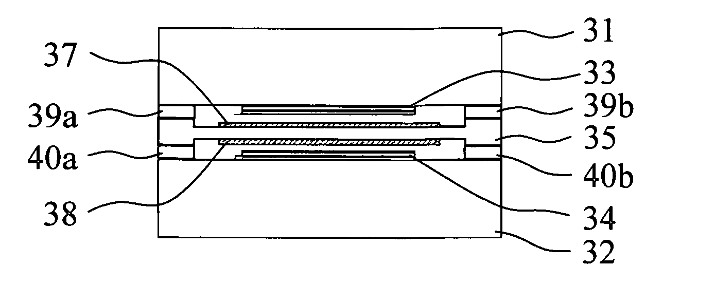
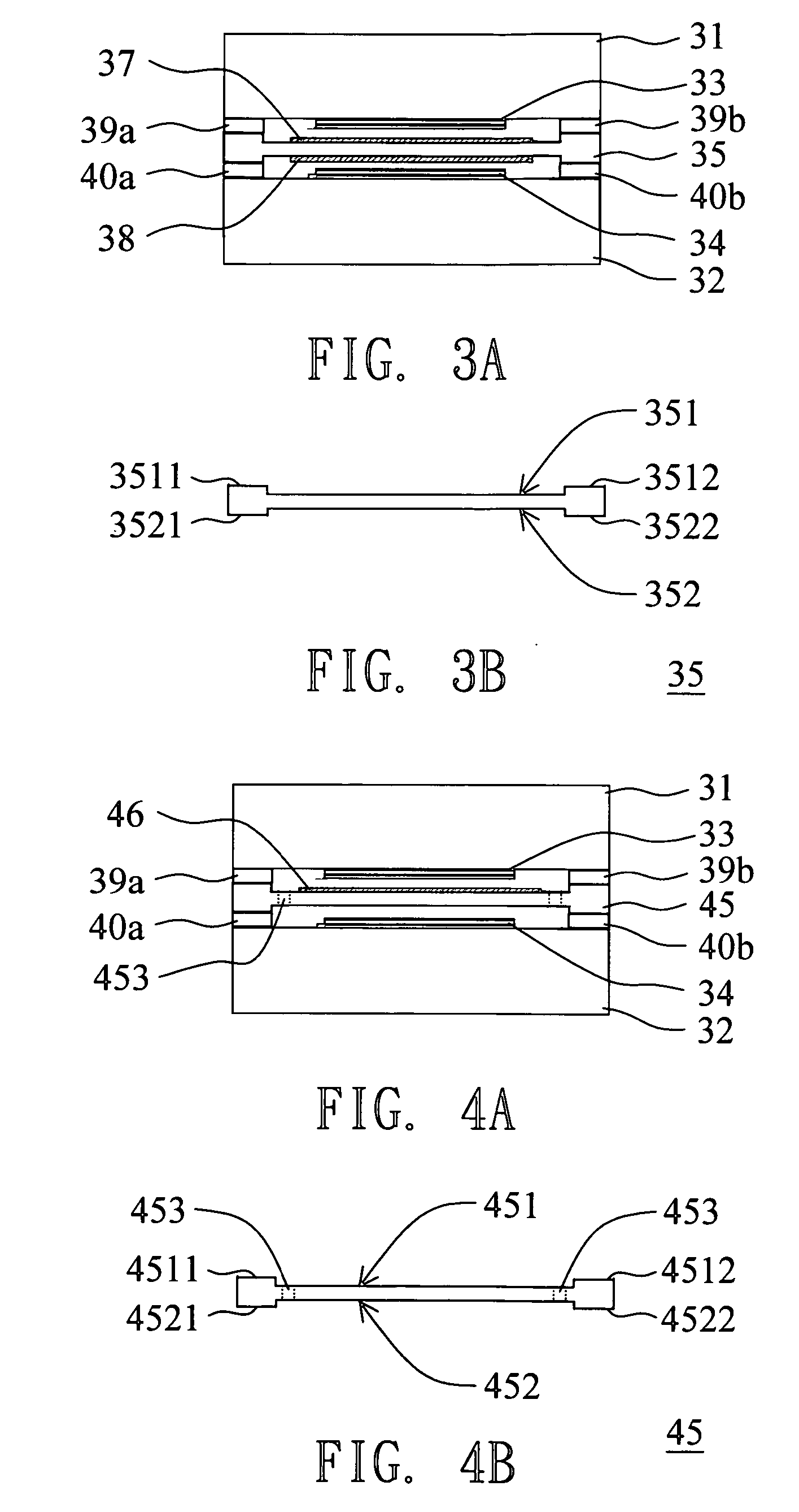
[0028]FIG. 3A illustrates an encapsulation structure of double sided organic light emitting device (OLED) according to the first embodiment of the present invention. In the first embodiment, the encapsulation structure comprises a first substrate 31, a second substrate 32, a first OLED 33, a second OLED 34, a supporter 35, a first moisture absorption layer 37 and a second moisture absorption layer 38. The first substrate 31 and the second substrate 32 are disposed oppositely. The first OLED 33 is disposed on the first substrate 31. The second OLED 34 is disposed on the second substrate 32, and opposite to the first OLED 33. The supporter 35 is disposed between the first OLED 33 and the second OLED 34.

[0029]FIG. 3B illustrates the supporter according to the first embodiment of the present invention. The supporter 35 has a first surface 351 and a second surface 352. The first moisture absorption layer 37 and the second moisture absorption layer 38 are disposed on the first surface 35...

second embodiment

[0033]FIG. 4A illustrates an encapsulation structure of double sided organic light emitting device (OLED) according to the second embodiment of the present invention. Components common to FIG. 3A retain the same numeric designation. FIG. 4B illustrates the supporter according to the second embodiment of the present invention.

[0034] In the second embodiment, the encapsulation structure comprises a first substrate 31, a second substrate 32, a first OLED 33, a second OLED 34, a supporter 45 and a moisture absorption layer 46. The first substrate 31 and the second substrate 32 are disposed oppositely. The first OLED 33 is disposed on the first substrate 31. The second OLED 34 is disposed on the second substrate 32, and opposite to the first OLED 33. The supporter 45 is disposed between the first OLED 33 and the second OLED 34.

[0035] The supporter 45, having a first surface 451 and a second surface 452, comprises at least a through hole penetrated from the first surface 451 to the seco...

third embodiment

[0038]FIG. 5 illustrates an encapsulation structure of double sided organic light emitting device (OLED) according to the third embodiment of the present invention. Components common to FIG. 3A retain the same numeric designation.

[0039] The major difference between the third and first embodiments is that the supporter 55 is wider than the first substrate 31 and the second substrate 32. Also, the exterior side of the supporter 55 is not thicker than (ex. about the same thickness with) the overall structure after the encapsulation is completed. Accordingly, the supporter design of the third embodiment not only prevents the direct touch between the OLED and the moisture absorption layer, but also increases the strengths of the encapsulation structure.

[0040] According to the encapsulation structures disclosed in the first, second and third embodiments, the first sealing glues 39a, 39b and the second sealing glues 40a, 40b each can be controlled in a thickness of about (even less than)...


PUM


Abstract

An encapsulation structure of double sided organic light emitting device (OLED) comprises a first substrate and a second substrate disposed oppositely; a first organic light emitting device (OLED) disposed on the first substrate; a second OLED disposed on the second substrate; a supporter disposed between the first OLED and the second OLED; and at least a moisture absorption layer disposed at the supporter for absorbing moisture inside the encapsulation structure.

Description

[0001] This application claims the benefit of Taiwan application Ser. No. 094142672, filed Dec. 2, 2005, the subject matter of which is incorporated herein by reference. BACKGROUND OF THE INVENTION [0002] 1. Field of the Invention [0003] The invention relates in general to an encapsulation structure of double sided organic light emitting device (OLED) and method of fabricating the same, and more particularly to a compact encapsulation structure of OLED being resistant to moisture and present a compact appearance. [0004] 2. Description of the Related Art [0005] Use of organic light emitting device (OLED) in the flat panel displays possesses several competitive advantages, such as self illumination, high brightness, wide viewing angle, vivid contrast, quick response, broad range of operating temperature, high luminous efficiency and uncomplicated process of fabrication. Thus, the OLED represents a promising technology for display applications and has receives the worldwide attention i...

Claims


Application Information

Patent Timeline
IPC IPC(8): H05B33/04
CPCH01L25/048H01L27/3267H01L27/3286H01L51/524H01L51/5259H01L2924/0002H10K59/90H10K59/128H10K59/176H10K50/846H10K50/841H01L2924/00
Inventor CHAO, CHING-IAN
Owner AU OPTRONICS CORP
Why Eureka
Try Eureka