Hybrid OLED having phosphorescent and fluorescent emitters

a hybrid oled and fluorescent technology, applied in the field of hybrid oleds with fluorescent and fluorescent emitters, can solve the problems of limited operation stability of oleds

Active Publication Date: 2006-10-19
UNIVERSAL DISPLAY
View PDF69 Cites 195 Cited by
  • Summary
  • Abstract
  • Description
  • Claims
  • Application Information

AI Technical Summary

Problems solved by technology

White OLEDs having only phosphorescent emissive materials may be highly efficient, but their

Method used


Image

  • Hybrid OLED having phosphorescent and fluorescent emitters
  • Hybrid OLED having phosphorescent and fluorescent emitters
  • Hybrid OLED having phosphorescent and fluorescent emitters

Examples


example 1

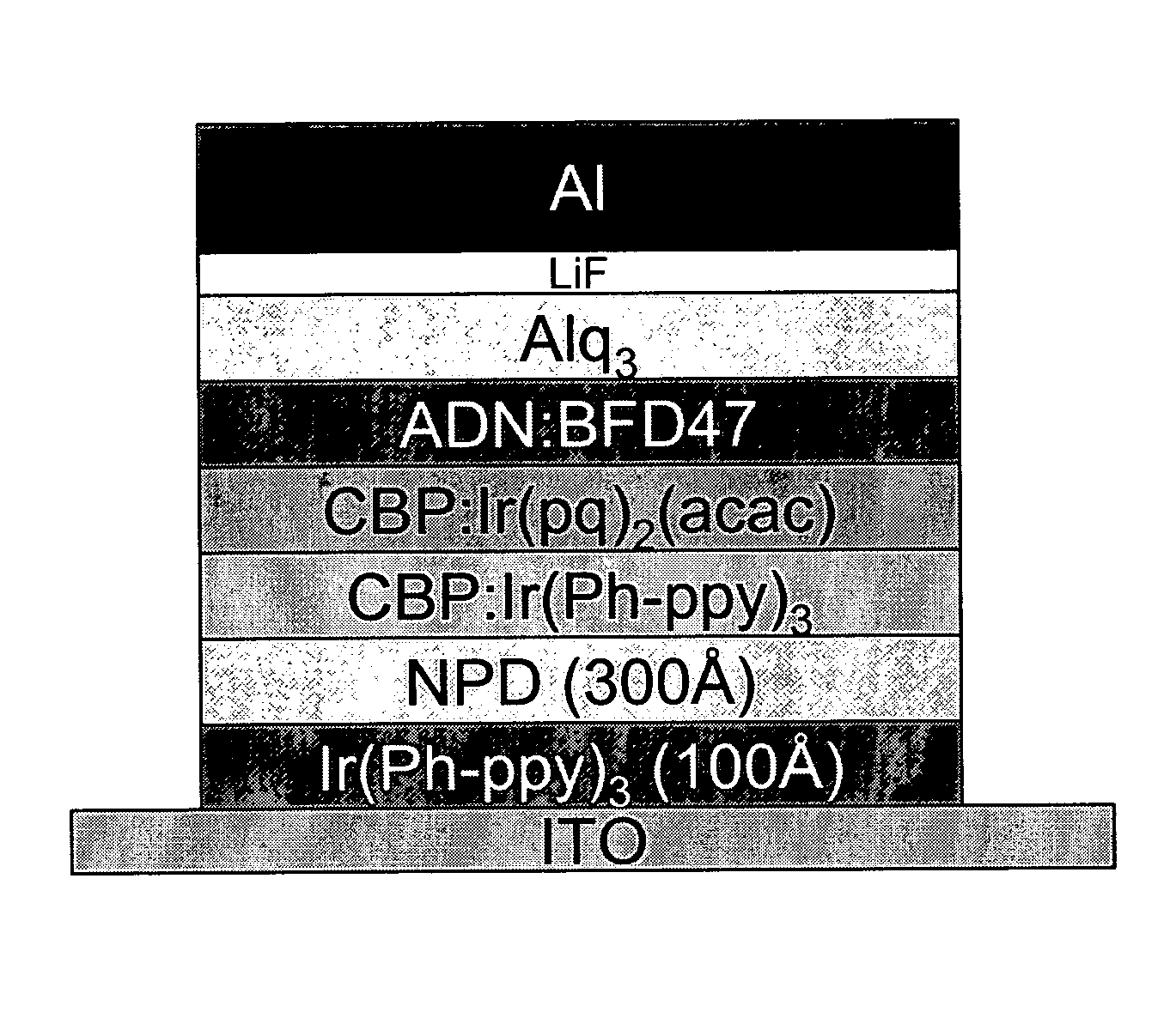
[0116] An OLED was prepared with the structure ITO / Ir(Ph-ppy)3(100 Å) / NPD(300 Å) / CBP:Ir(Ph-ppy)3 (75 Å,12%) / CBP:Ir(pq)2(acac) (25 Å,6%) / ADN:BFD47(300 Å,6%) / Alq3(300 Å) / LiF(5 Å) / Al(1000 Å). The device structure is depicted schematically in FIG. 3. FIG. 6 shows the plot of the external quantum efficiency versus current density for this device, which has a maximum external quantum efficiency of 4.7%. The plots of the normalized emission spectra at various current densities (brightness) are shown in FIG. 8. As can be seen in FIG. 8, the device shows a high color-stability of the light emission over a wide range of currents or luminances.

example 2

[0117] An OLED was prepared with the structure ITO / Ir(Ph-ppy)3 (100 Å) / NPD(300 Å) / CBP:Ir(Ph-ppy)3(75 Å,9%) / CBP:Ir(pq)2(acac)(25 Å,6%) / ADN:BFD47(200 Å,6%) / Alq3(400 Å) / LiF(5 Å) / Al(1000 Å). The device structure is depicted schematically in FIG. 3. FIG. 6 shows the plot of the external quantum efficiency versus current density for this device, which has a maximum external quantum efficiency of 4.7%.

example 3

[0118] An OLED was prepared with the structure ITO / Ir(Ph-ppy)3(100 Å) / NPD(300 Å) / CBP:Ir(Ph-ppy)3(6%):Ir(pq)2(acac)(1%)(100 Å) / ADN:BFD47(300 Å,6%) / Alq3(300 Å) / LiF(5 Å) / Al(1000 Å). The device structure is depicted schematically in FIG. 4. FIG. 6 shows the plot of the external quantum efficiency versus current density for this device, which has a maximum external quantum efficiency of 5.4%.


PUM

PropertyMeasurementUnit
External quantum efficiencyaaaaaaaaaa
Electric potential / voltageaaaaaaaaaa

Abstract

The present invention provides organic light emitting devices having a combined emission from at least two emissive materials, a fluorescent blue emissive material and a phosphorescent emissive material. The device may further comprise additional fluorescent or phosphorescent emissive materials. In preferred embodiments, the invention provides OLEDs having three different emissive materials—a red emissive material, a green emissive material and a blue emissive material. The invention provides a device architecture which is optimized for efficiency and lifetime by using a combination of fluorescent and phosphorescent emitters. Further, in preferred embodiments the device architecture provides a high color-stability of the light emission over a wide range of currents or luminances.

Description

FIELD OF THE INVENTION [0001] The present invention relates to organic light emitting devices (OLEDs), and more specifically to OLEDS that emit light using a combination of fluorescent emitters and phosphorescent emitters. In preferred embodiments the combined emission from the fluorescent and phosphorescent emitters sufficiently span the visible spectrum to give a white emission. BACKGROUND [0002] Opto-electronic devices that make use of organic materials are becoming increasingly desirable for a number of reasons. Many of the materials used to make such devices are relatively inexpensive, so organic opto-electronic devices have the potential for cost advantages over inorganic devices. In addition, the inherent properties of organic materials, such as their flexibility, may make them well suited for particular applications such as fabrication on a flexible substrate. Examples of organic opto-electronic devices include organic light emitting devices (OLEDs), organic phototransistors...

Claims


Application Information

Patent Timeline
IPC IPC(8): H01L51/54H05B33/14
CPCC09K11/06C09K2211/1011H01L51/0054H01L51/0058H01L51/006H01L51/0071H01L2251/5376H01L51/0085H01L51/5016H05B33/14H01L51/504H01L51/5044H01L51/0081H10K85/622H10K85/626H10K85/633H10K85/657H10K85/324H10K85/342H10K50/131H10K50/11H10K2101/10H10K50/13H10K2101/27H10K50/15H10K50/19H10K59/32H10K85/615H10K85/6572H10K2101/40H10K2101/30H10K2102/351
Inventor TUNG, YEH-JIUNWEAVER, MICHAEL S.HACK, MICHAELESLER, JAMES
Owner UNIVERSAL DISPLAY
Why Eureka
Try Eureka