Flat panel display, fabricating method thereof, fabricating apparatus thereof, picture quality controlling method thereof, picture quality controlling apparatus

a technology of flat panel display and fabricating method, applied in the field of flat panel display, can solve the problems of heavy weight and bulky volume of cathode ray tubes, and achieve the effect of reducing the amount of material used, and improving the quality of the finished produ

Active Publication Date: 2007-06-07
LG DISPLAY CO LTD
View PDF5 Cites 59 Cited by
  • Summary
  • Abstract
  • Description
  • Claims
  • Application Information

AI Technical Summary

Benefits of technology

[0034] A method of controlling a picture quality of a flat panel display according to other embodiment in the method of controlling the picture quality of the flat panel display panel having a link pixel such that a plurality of data lines and a plurality of scan lines are cross each other, a plurality of pixels are arranged, and a defective pixel is electrically connected to a normal pixel adjacently with thereof, comprises the steps of storing a location data for indicating a location of the link pixel and a compensation data for compensating a charging characteristics of the link pixel into a memory; and modulating the location data and a digital video data to be displayed at the link pixel on the basis of the location data and the compensation data.
[0035] A picture quality controlling apparatus of a flat panel display according to another embodiment, in the method of controlling the picture quality of the flat panel display panel having a link pixel such that a plurality of data lines and a plurality of scan lines are crossed each other, a plurality of pixels are arranged, and a defective pixel is electrically connected to a normal pixel adjacently with thereof, comprises a memory that stores a location data that indicates a location of the link pixel and a compensation data for compensating a charging characteristics of the link pixel into a memory. A compensation circuit that modulates the location data and a digital video data to be displayed at the link pixel on the basis of the location data and the compensation data.

Problems solved by technology

Cathode Ray Tubes were conventionally used but have a heavy weight and a bulky volume.

Method used


Image

  • Flat panel display, fabricating method thereof, fabricating apparatus thereof, picture quality controlling method thereof, picture quality controlling apparatus
  • Flat panel display, fabricating method thereof, fabricating apparatus thereof, picture quality controlling method thereof, picture quality controlling apparatus
  • Flat panel display, fabricating method thereof, fabricating apparatus thereof, picture quality controlling method thereof, picture quality controlling apparatus

Examples


first embodiment

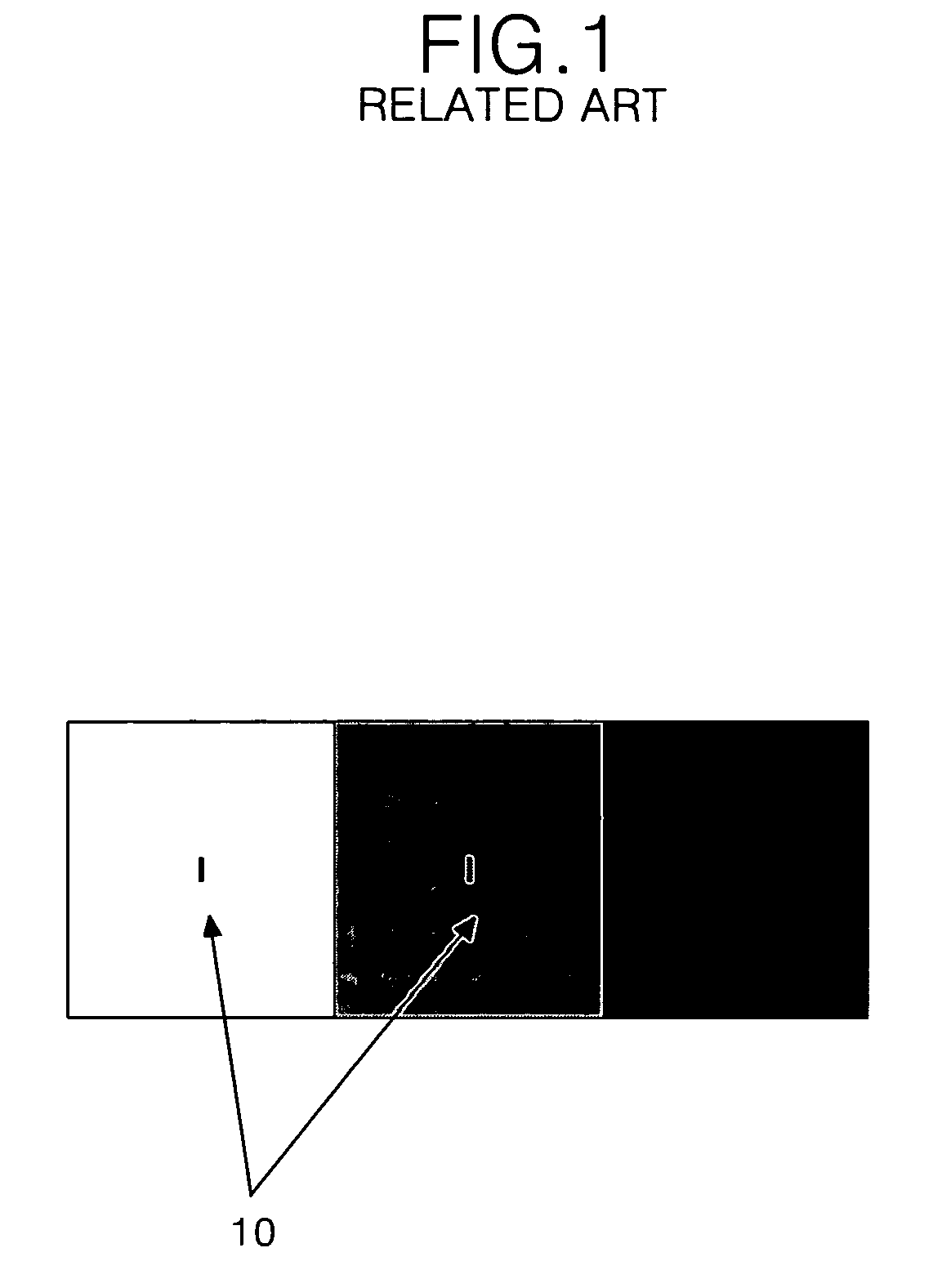
[0076]FIG. 4 and FIG. 5 are diagrams that explain a repairing process of a TN mode liquid crystal display device according to the present invention.

[0077] Referring to FIG. 4 and FIG. 5, in the repairing process, a link pattern 44 is directly formed on the a pixel electrode 43A of the adjacently defective pixel 10 and a pixel electrode 43B of the normal pixel 11 by using the W-CVD (Chemical Vapor Deposition) process.

[0078] A gate line 41 and a data line 42 cross each other on a glass substrate 45 of a lower substrate and a TFT is formed at an intersection thereof. A gate electrode of the TFT is electrically connected to the gate line 41 and a source electrode is electrically connected to the data line 42. A drain electrode of the TFT is electrically connected, via a contact hole, to the pixel electrodes 43A and 43B.

[0079] A gate metal pattern includes the gate line 41 and the gate electrode of the TFT formed on the glass substrate 45 by a gate metal deposition process such as alum...

second embodiment

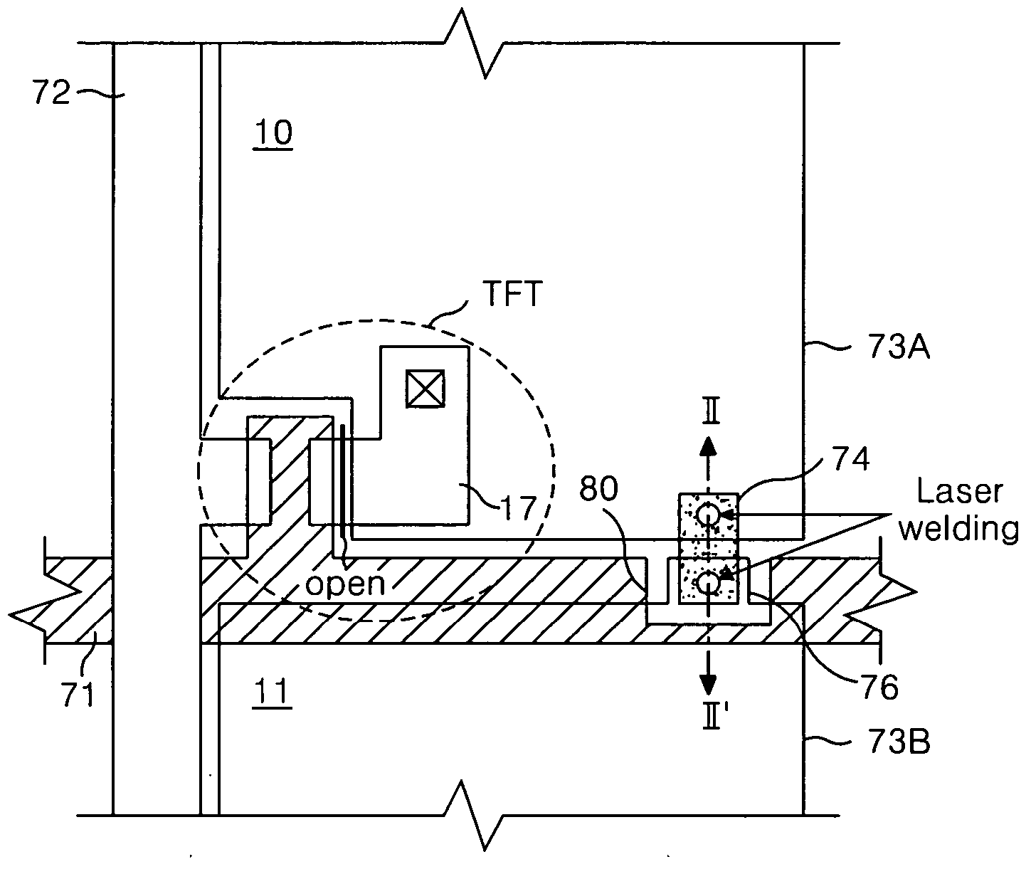
[0085]FIG. 7 and FIG. 8 are diagrams for explaining a repairing process of a TN mode liquid crystal display device according to the present invention.

[0086] Referring to FIG. 7 and FIG. 8, the repairing process includes a link pattern 74 that overlaps with a pixel electrode 73A of the defective pixel 10 and a pixel electrode 73B of the normal pixel 11 adjacently with thereof with having a protective film 77 therebetween.

[0087] A gate line 71 and a data line 72 cross each other on a glass substrate 75 of a lower substrate and a TFT is formed at an intersection thereof. A gate electrode of the TFT is electrically connected to the gate line 71 and a source electrode is electrically connected to the data line 72. A drain electrode of the TFT is electrically connected, via a contact hole, to the pixel electrodes 73A and 73B.

[0088] A gate metal pattern that includes the gate line 71 and the gate electrode of the TFT is formed on the glass substrate 75 by a gate metal deposition process,...

third embodiment

[0096]FIG. 10 and FIG. 11 are diagrams that explain a repairing process of an IPS mode liquid crystal display device according to the present invention.

[0097] Referring to FIG. 10 and FIG. 11, in the repairing process a link pattern 104 is directly formed on a pixel electrode 103A of the adjacent defective pixel 10 and a pixel electrode 103B of the normal pixel 11 by the W-CVD (Chemical Vapor Deposition) process.

[0098] A gate line 101 and a data line 102 cross each other on a glass substrate 105 of a lower substrate and a TFT is formed at an intersection thereof. A gate electrode of the TFT is electrically connected to the gate line 41 and a source electrode is electrically connected to the data line 42. A drain electrode of the TFT is electrically connected, via a contact hole, to the pixel electrodes 103A and 103B.

[0099] A gate metal pattern that includes the gate line 101, the gate electrode of the TFT and a common electrode 108 is formed on the glass substrate 105 by the gate ...


PUM

PropertyMeasurementUnit
Ri/Gi/Biaaaaaaaaaa
coloraaaaaaaaaa
areaaaaaaaaaaa

Abstract

A flat panel display, a fabricating method thereof, a fabricating apparatus thereof, a picture quality controlling method thereof and a picture quality controlling apparatus for reducing a recognizing degree of a defective pixel and electrically compensating a charging characteristics of the defective pixel are provided. In the flat panel display, a display panel has a plurality of pixels. A defective pixel is electrically connected to an adjacent normal pixel. A memory stores a location data that indicates a location of the link pixel and a compensation data that compensates for charging characteristics of the link pixel. A compensation circuit modulates a digital video data to be displayed on the link pixel on the basis of the location data and the compensation data.

Description

[0001] This application claims the benefit of Korean Patent Application No. P2005-0117064 filed in Korea on Dec. 2, 2005, which is hereby incorporated by reference. BACKGROUND [0002] 1. Field [0003] A flat panel display, and more particularly a flat panel display, a fabricating method thereof, a fabricating apparatus thereof, a picture quality controlling method thereof and a picture quality controlling apparatus are provided. [0004] 2. Related Art [0005] Recently, display devices have become increasingly popular as a visual information communicating media in information society. Cathode Ray Tubes were conventionally used but have a heavy weight and a bulky volume. Various flat panel display devices have been developed that can overcome the limit of such a cathode ray tube. [0006] Such flat panel displays include, for example, a liquid crystal display (LCD), a field emission display (FED), a plasma display panel (PDP) and an organic light emitting diode (OLED). Most of these devices...

Claims


Application Information

Patent Timeline
Patent Type & Authority Applications(United States)
IPC IPC(8): G01R31/00G02F1/133G02F1/1343G02F1/1368G09F9/00G09G3/20G09G3/30G09G3/36
CPCG09G3/006G09G3/3648G09G2330/10G09G3/20G09G3/30G09G3/296G09G3/36
Inventor CHUNG, IN JAEYOO, SOON SUNGNAM, SEUNG HEELEE, DEUK SUHWANG, JONG HEE
Owner LG DISPLAY CO LTD
Why Eureka
Try Eureka