
Systems and methods for LBIST testing using isolatable scan chains

a technology of scan chain and scan chain, which is applied in the field of systems and methods for lbist testing using isolatable scan chain, can solve the problems of increasing the chances of defects that may impair or impede the proper operation of the device, prohibitively expensive to take the deterministic approach, and increasing the complexity of digital devices

Active Publication Date: 2007-06-07
TOSHIBA ELECTRONICS DEVICES & STORAGE CORPORARTION +1
View PDF14 Cites 16 Cited by
  • Summary
  • Abstract
  • Description
  • Claims
  • Application Information

AI Technical Summary

Benefits of technology

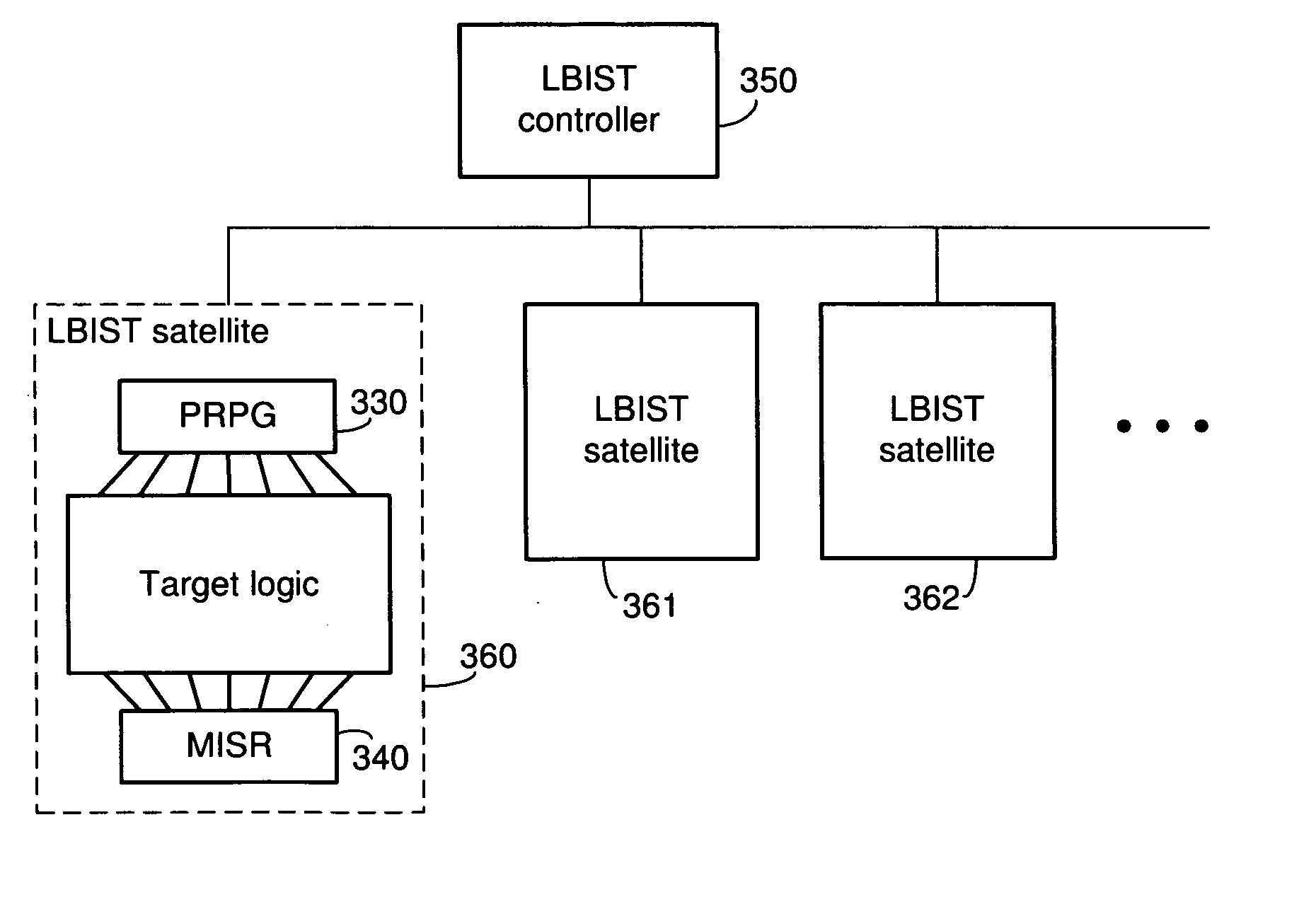
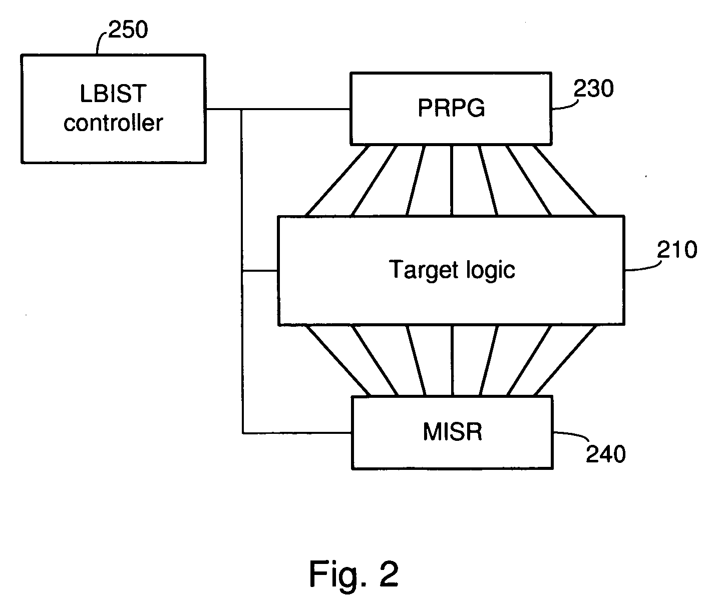
The invention is about a system and method for performing logic built-in self-tests (LBISTs) in digital circuits. The LBIST circuitry includes scan chains that are interposed with the target logic of the device under test. The scan chains are configured so that the last scan chain of one portion is coupled to the first scan chain of a succeeding portion. This allows for isolation of malfunctioning portions of the target logic without corrupting the data in other parts of the circuit. The testing of isolated processor cores can be performed initially to determine whether any of them are malfunctioning, and then the remaining processor cores can be tested in conjunction with the supporting functional blocks of the device. The LBIST circuitry can be isolated in each functional block and selectively coupled or decoupled with the boundary scan chains of other functional blocks using AND gates. The invention provides a way to efficiently and accurately test complex digital circuits.

Problems solved by technology

Digital devices are becoming increasingly complex.
As the complexity of these devices increases, there are more and more chances for defects that may impair or impede proper operation of the devices.
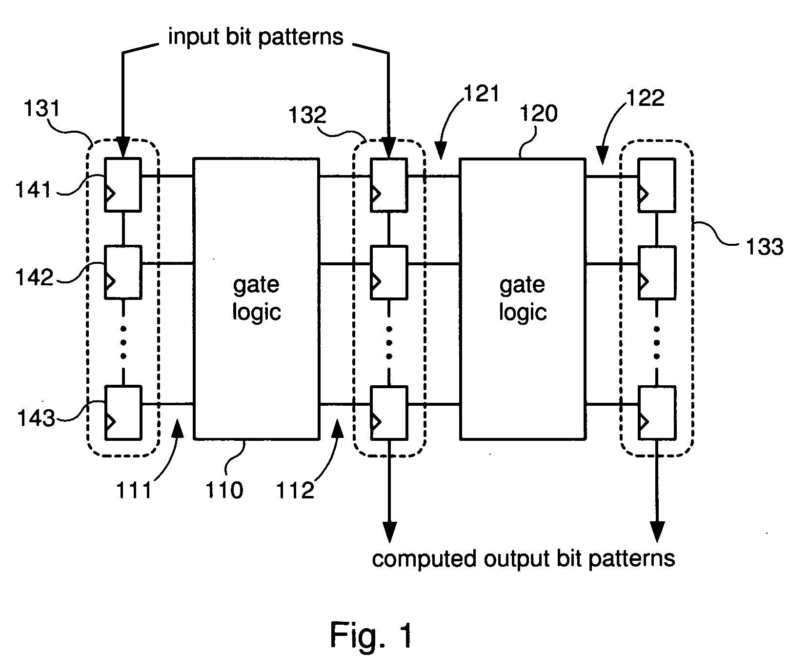
Because of the complexity of most devices, however, it would be prohibitively expensive to take the deterministic approach of testing every possible combination of inputs to each logic gate and states of the device.
While this testing approach can be very effective, it does have some drawbacks.
Any errors that are produced during testing are combined with other data, and possibly other errors, in the MISR, so it cannot be determined whether the errors arose in a single functional block (e.g. processor) or multiple blocks, or which if the functional blocks caused the error(s).

Method used


Image

  • Systems and methods for LBIST testing using isolatable scan chains
  • Systems and methods for LBIST testing using isolatable scan chains
  • Systems and methods for LBIST testing using isolatable scan chains

Examples


Embodiment Construction

[0024] One or more embodiments of the invention are described below. It should be noted that these and any other embodiments described below are exemplary and are intended to be illustrative of the invention rather than limiting.

[0025] As described herein, various embodiments of the invention comprise systems and methods for performing logic built-in self-tests (LBISTs) in digital circuits, where individual functional blocks (e.g., processor cores) can be isolated to localize errors generated during testing and prevent the errors from corrupting test data generated in other functional blocks.

[0026] In one embodiment, a STUMPS-type LBIST architecture is implemented in a device under test. The LBIST circuitry includes a set of scan chains that are interposed with the target logic of the device under test. The scan chains are configured so that the last scan chain of one portion is coupled to the first scan chain of a succeeding portion. These first / last scan chains are referred to h...


PUM


Abstract

Systems and methods for performing logic built-in self-tests (LBISTs) in digital circuits, where boundary scan chains in functional blocks of the circuits can be selectively coupled / decoupled to isolate the functional blocks during LBIST testing. In one embodiment, processor cores of a multiprocessor chip are isolated and LBIST testing is performed to determine whether any of the processor cores is malfunctioning. If none of the processor cores malfunctions, the processor cores are tested in conjunction with the supporting functional blocks of the device to determine whether the multiprocessor is fully functional. If one or more processor cores malfunctions, these processor cores are isolated and the remaining processor cores are tested in conjunction with the supporting functional blocks of the device to determine whether the multiprocessor operates properly with reduced functionality.

Description

BACKGROUND [0001] 1. Field of the Invention [0002] The invention relates generally to the testing of electronic circuits, and more particularly to systems and methods for performing logic built-in self-tests (LBISTs) using circuitry that enables the isolation of scan chains in selected portions of the functional logic of a device under test. [0003] 2. Related Art [0004] Digital devices are becoming increasingly complex. As the complexity of these devices increases, there are more and more chances for defects that may impair or impede proper operation of the devices. The testing of these devices is therefore becoming increasingly important. [0005] Testing of a device may be important at various stages, including in the design of the device, in the manufacturing of the device, and in the operation of the device. Testing at the design stage ensures that the design is conceptually sound. Testing during the manufacturing stage may be performed to ensure that the timing, proper operation ...

Claims


Application Information

Patent Timeline
Patent Type & Authority Applications(United States)
IPC IPC(8): G01R31/28
CPCG01R31/318536
Inventor KIRYU, NAOKIRILEY, MACK WAYNECHELSTROM, NATHAN PAUL
Owner TOSHIBA ELECTRONICS DEVICES & STORAGE CORPORARTION
Learn More