SOI active layer with different surface orientation

a technology of active layer and surface orientation, applied in the direction of semiconductor/solid-state device manufacturing, basic electric elements, electric devices, etc., can solve the problems of non-epitaxial silicon growth on unwanted areas, difficult to maintain a clean surface on which and difficult to selectively grow epitaxial silicon

Inactive Publication Date: 2007-06-14
NORTH STAR INNOVATIONS
View PDF7 Cites 44 Cited by
  • Summary
  • Abstract
  • Description
  • Claims
  • Application Information

AI Technical Summary

Problems solved by technology

However, the selectively epitaxially grown silicon may include defects in the subsequently epitaxially grown silicon active layer e.g. at a boundary of the epitaxially grown silicon.
Also, maintaining a clean surface on which to selectively grow the epitaxial silicon may be difficult due to different materials

Method used


Image

  • SOI active layer with different surface orientation
  • SOI active layer with different surface orientation
  • SOI active layer with different surface orientation

Examples


Embodiment Construction

[0012] The following sets forth a detailed description of a mode for carrying out the invention. The description is intended to be illustrative of the invention and should not be taken to be limiting.

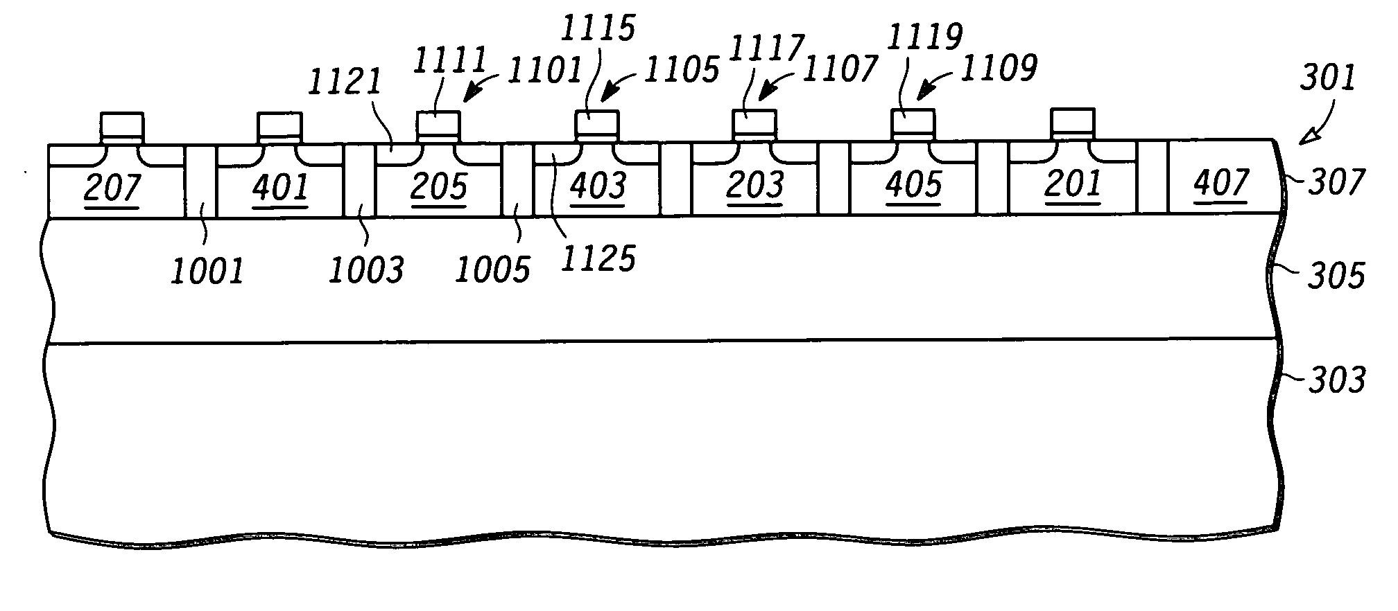
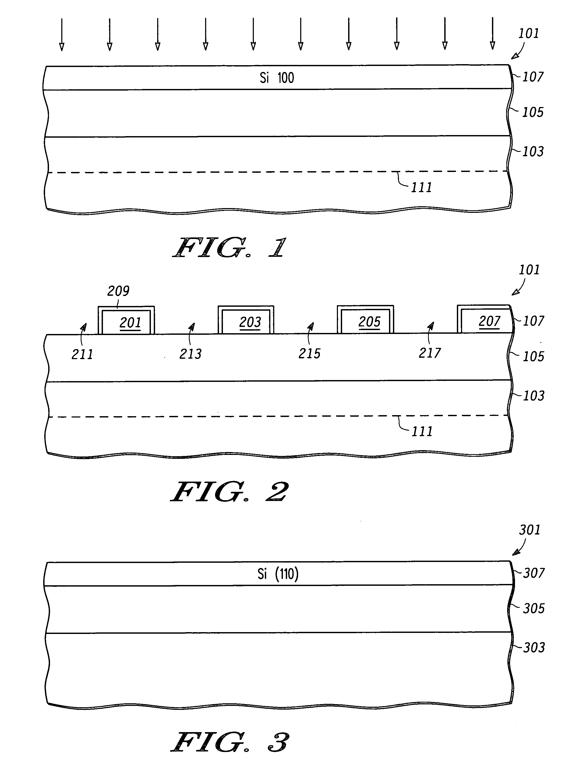
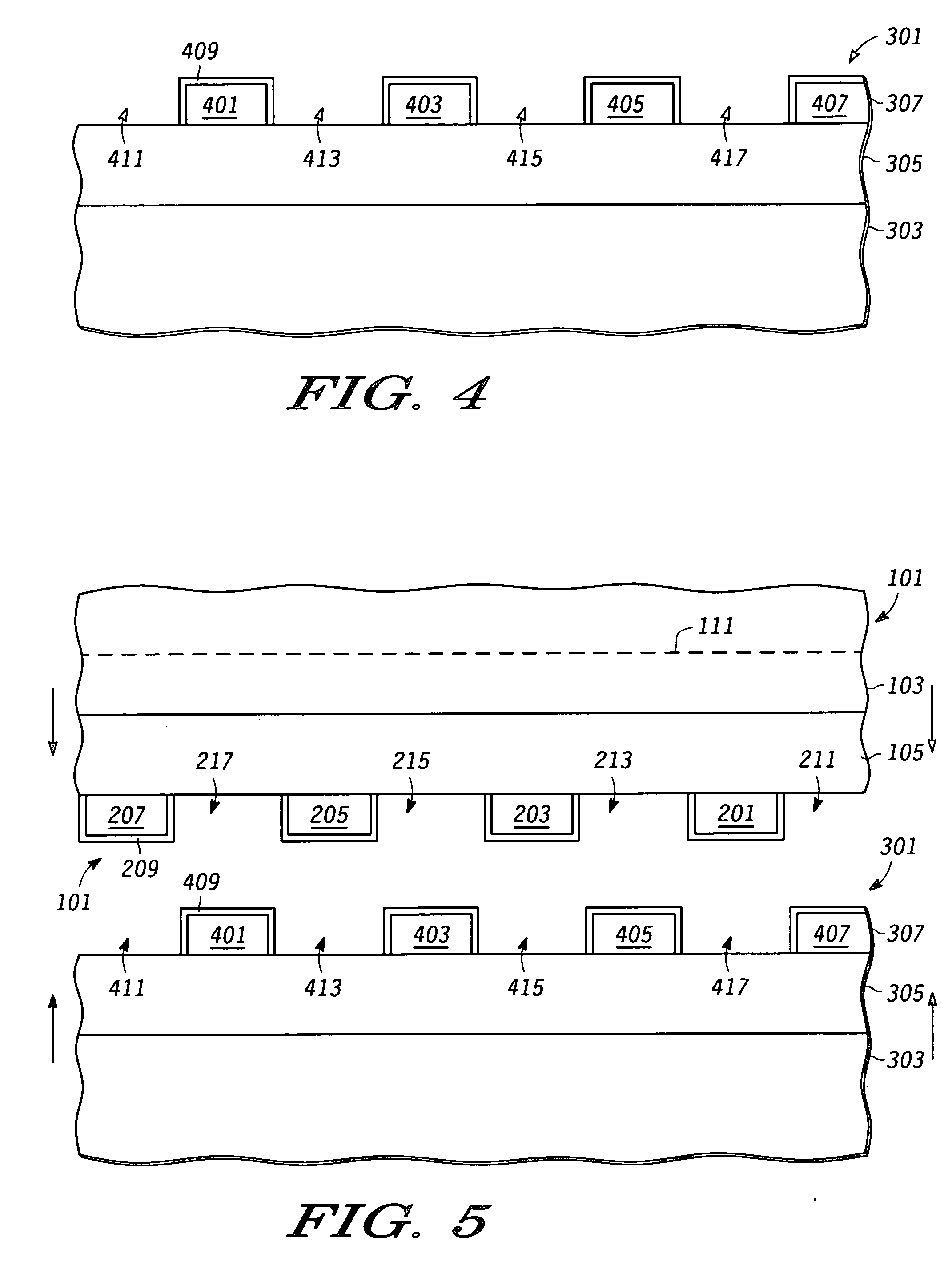
[0013]FIG. 1 is a partial cross sectional side view of a wafer utilized to form semiconductor structures having a particular surface orientation that will be located between areas of semiconductors structures of a second surface orientation of a second wafer to provide a resultant layer having structures of a first surface orientation and structures of a second surface orientation.

[0014] Wafer 101 has an SOI configuration with an active semiconductor layer (e.g. silicon, silicon germanium) 107 having a surface orientation (100). Layer 107 is on an insulator layer 105 (e.g. silicon oxide). Layer 105 is on substrate layer 103 (e.g. monocrystalline silicon). As shown in FIG. 1, hydrogen ions are implanted into substrate layer 103 to form a damaged region 111 that will be utilized in subs...


PUM


Abstract

A wafer having an SOI configuration and active regions having different surface orientations for different channel type transistors. In one example, semiconductor structures having a first surface orientation are formed on a donor wafer. Semiconductor structures having a second surface orientation are formed on a second wafer. Receptor openings are formed on the second wafer. The semiconductor structures having the first surface orientation are located in the receptor openings and transferred to the second wafer. The resultant wafer has semiconductor regions having a first surface orientation for a first channel type of transistor and semiconductor regions having a second surface orientation for a second channel type transistor.

Description

BACKGROUND OF THE INVENTION [0001] 1. Field of the Invention [0002] This invention relates in general to semiconductor devices and more particularly to devices implemented with semiconductor on insulator (SOI) technology. [0003] 2. Description of the Related Art [0004] The surface orientation of a semiconductor material is descriptive of the lattice orientation of the material at the surface of the material. With some semiconductor circuits, it may be desirable to implement the P-channel transistors and N-channel transistors in semiconductor active regions having different surface orientations. For example, some N-channel transistors have a relatively higher electron mobility in silicon having a surface orientation (100) as opposed to the electron mobility of an N-channel transistor in silicon with a surface orientation (110). On the other hand, some P-channel transistors will have a higher hole mobility with their channels being implemented in silicon having a surface orientation (...

Claims


Application Information

Patent Timeline
IPC IPC(8): H01L21/00
CPCH01L21/76254H01L21/02002H01L21/20
Inventor ADETUTU, OLUBUNMI O.JONES, ROBERT E.WHITE, TED R.
Owner NORTH STAR INNOVATIONS
Why Eureka
Try Eureka