Single-ended CMOS signal interface to differential signal receiver loads

a signal interface and receiver technology, applied in the direction of voltage/current interference elimination, pulse technique, reliability increasing modifications, etc., can solve the problems of signal delay, output signal from the cmos circuit can also experience a mismatch or phase shift or misalignment with the lvds load, price increase, etc., to achieve lower delay, less jitter, and lower cost

Inactive Publication Date: 2007-06-21
LSI CORPORATION
View PDF5 Cites 10 Cited by
  • Summary
  • Abstract
  • Description
  • Claims
  • Application Information

AI Technical Summary

Benefits of technology

[0007] It is therefore one aspect of the present invention to provide for an improved interface of a single-ended CMOS type signal to differential signal loads.
[0008] It is therefore one aspect of the present invention to provide an interface that will convert a single-ended CMOS signal to differential signaling for differential signal loads, thus resulting in lower cost, lower delay and less jitter, yet producing higher bandwidth and low phase-offset.

Problems solved by technology

The problem with the circuit shown in FIG. 1 is that the use of a positive and negative driver can cause a signaling delay.
The output signal from the CMOS circuit can also experience a mismatch or phase shift or misalignment with the LVDS load during signaling.
Furthermore, the design in FIG. 1 will cause a price increase because of the introduction of additional logic to accomplish the conversion from a single ended input to the differential output.

Method used


Image

  • Single-ended CMOS signal interface to differential signal receiver loads
  • Single-ended CMOS signal interface to differential signal receiver loads

Examples


Embodiment Construction

[0014] The particular values and configurations discussed in these non-limiting examples can be varied and are cited merely to illustrate embodiments of the present invention and are not intended to limit the scope of the invention.

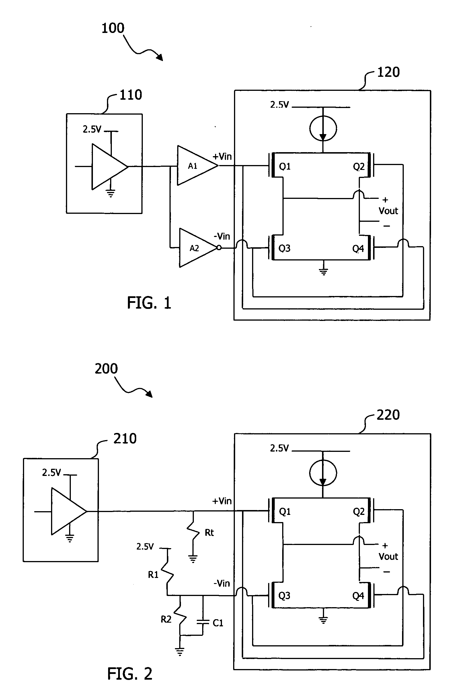
[0015] As stated in the background, the introduction positive and negative drivers between CMOS and LVDS loads can cause a signaling delay. The output signal from the CMOS circuit can also experience a mismatch or phase shift or misalignment with the LVDS load during signaling.

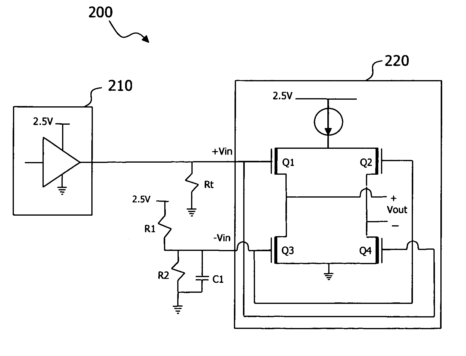
[0016] Referring to FIG. 2, a simplified circuit 200 illustrates a solution to problems previously encountered by CMOS to differential circuit interfaces. The solution introduces two resistors, labeled R1 and R2, and a capacitor, C1, in place of the two amplifiers. The three circuit elements, R1, R2 and C1, are used to fix the voltage on the negative input of the LVDS. When the negative input on the LVDS is fixed at a certain bias voltage, then the LVDS input will receive the diff...


PUM


Abstract

The interface of a single-ended CMOS type signal to differential signal loads includes a LVDS load having a +Vin input and a −Vin input, a CMOS circuit having an output signal line, and a resistor Rt connected to the output signal line and ground. A 2.5 volt source line is connected through a resistor R1 to the −Vin input of the LVDS load, the output signal line is connected directly to the +Vin input of the LVDS load, and a resistor R2 and capacitor C1 re connected in parallel between R1 and the −Vin input and ground.

Description

FIELD OF THE INVENTION [0001] The present invention is generally related to signal drivers and receivers as used in the communications industry. More particularly, the present invention is related to the interface that will convert a single-ended CMOS signal to differential signaling for differential signal loads, thus resulting in lower cost, lower delay and less jitter, yet producing higher bandwidth and low phase-offset. BACKGROUND [0002] Drivers are used in communications. Because different circuits utilize different drivers for the transmitters and receivers, it is necessary to interface diverse driver types with varying loads. All drivers have different voltage swings and load end termination. Because there are so many types of communications drivers, there is a need for drivers that can interface with varying loads. [0003] Delays are experienced whenever a single-ended signal, such as a CMOS signal output, is interfaced with a differential signal, such as an LVDS or PCML rece...

Claims


Application Information

Patent Timeline
Patent Type & Authority Applications(United States)
IPC IPC(8): H03K19/094
CPCH03K19/00361H03K19/018528
Inventor TANG, GEORGE
Owner LSI CORPORATION
Why Eureka
Try Eureka