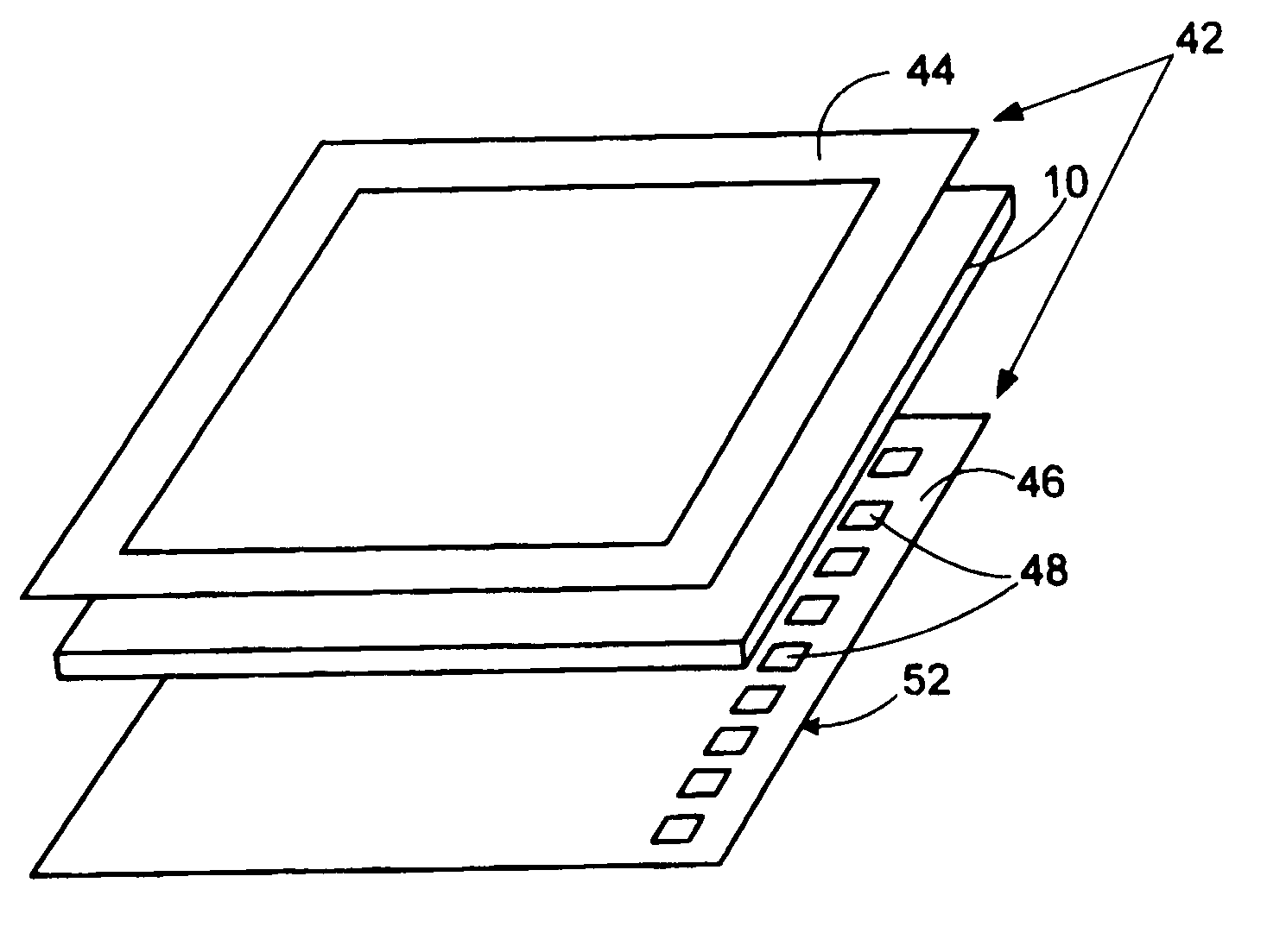
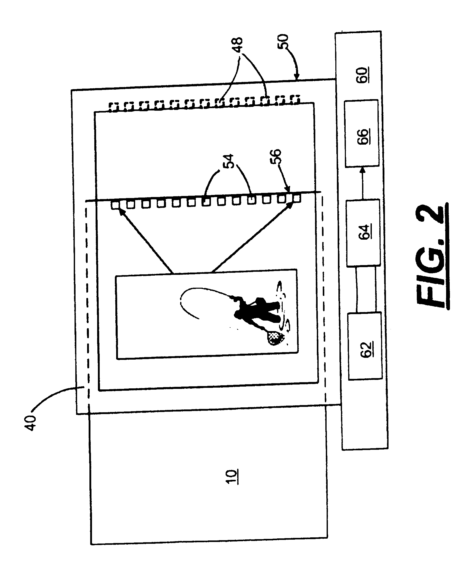
[0015] As described in more detail below, one embodiment of the disclosure provides a system and method for providing improved EL signage and display systems. A pattern(s) may be printed on an EL substrate to provide, for example, a customized sign or display that is receivable into a separate frame (which might also be referred to, in some embodiments, as a sign or display holder). The pattern(s) may correspond to encoded information that enables a controller in the display holder to selectively illuminate portions of the sign. Since the system enables interchangeability of signs with the holder, a number of different signs may be used with a single sign holder enabling a user to quickly change the sign and its display options.
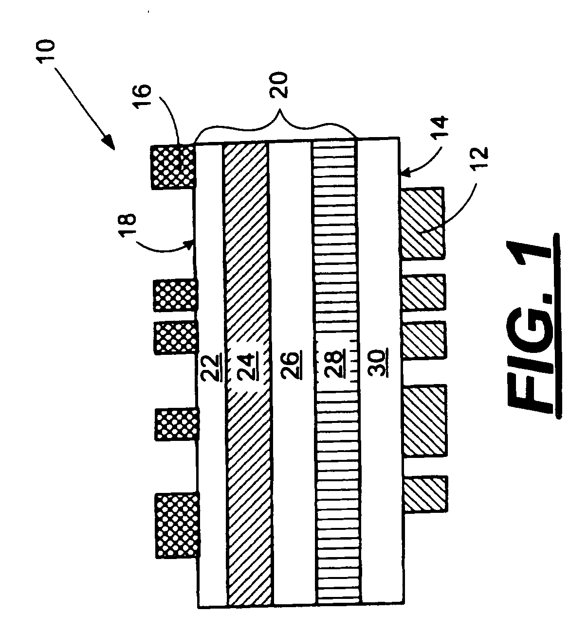
[0016] With reference to FIG. 1, there is provided a cross-sectional view of an EL signage 10 including an image pattern 12 printed adjacent (e.g., on) a first surface 14 thereof and a conductor pattern 16 printed adjacent (e.g., on) a second surface 18 thereof. The substrate 20 is an EL substrate. Current commercially available EL substrates 20 typically include an insulative or dielectric layer 22, an EL material layer 24, a translucent conductor layer 26, and a translucent protective layer 28. An image receiving layer 30 may be applied to the translucent protective layer 28 to provide a suitable surface for receiving the image pattern 12.
[0017] In an exemplary embodiment, the image pattern 12 may be provided by an imaging substance, such as monochrome or color inks. Such a substance may be applied to the image receiving layer 30 using, for example, screen printing, rotogravure printing, flexographic printing, lithographic printing, laser printing, ink jet printing, and the like. More flexibility in applying an image to the image receiving layer 30 may be provided by ink jet printing as described in U.S. Publication No. 2002/0090495.
[0018] The conductor pattern 16 applied to the dielectric layer 22 may likewise be applied by a wide variety of printing techniques including, but not limited to, vacuum deposition, chemical vapor deposition, electroplating, screen printing, rotogravure printing, flexographic printing, lithographic printing, and ink jet printing. The conductive pattern 16 may be a single conductive layer or, as shown in FIG. 1, may be a particular conductor pattern on the dielectric layer 22. Conductive inks that may be used to provide the conductor pattern 16 by a printing method, include, but are not limited to inks containing copper, silver, or carbon particles. In order to provide increased flexibility for design and operation of the EL signage, a conductive ink may be applied by a micro-fluid ejection device. The thickness of the conductor pattern 16 may range from about 0.5 to about 5.0 microns. As described in more detail below, electrical contacts (e.g., contact pads) are provided in electrical communication with the conductor pattern 16 for connection to a frame, such as a sign holder.
[0019] The insulative or dielectric layer 22 typically has a thickness ranging from about 20 to about 200 microns and may be provided by a material having a dielectric constant at 20° C. of greater than about fifty. Suitable materials having relatively high dielectric constants include, but are not limited to, barium or strontium titanate dispersed in a polymeric material, and titanium dioxide dispersed in a polymeric material. A particularly suitable polymeric material for dispersing the barium, strontium, or titanium compounds is a fluoropolymer material such as poly(tetrafluoroethylene). Accordingly, a particularly suitable dielectric layer 22 includes barium titanate dispersed in a fluoropolymer layer.
[0020] The EL layer 24 may include organic and/or inorganic EL materials. Inorganic materials typically provide brighter luminous characteristics and may be selected from terbium-doped zinc sulfide (ZnS:Tb), manganese-doped zinc sulfide (ZnS:Mn), cerium-doped yttrium aluminum garnet (YAG:Ce), copper-doped zinc selenium sulfide (ZnSeS:Cu), europium-doped strontium barium silicon oxide (SrBaSiO4:Eu), cerium-doped strontium sulfide (SrS:Ce), copper-doped strontium sulfide (SrS:Cu), copper and silver-doped strontium sulfide (SrS:Cu,Ag), and the like. The thickness of the EL layer 24 may range from about 100 nanometers to about 5 microns.
[0021] The conductor layer 26 of the EL substrate 20 is typically made of a translucent conductive material such as indium tin oxide (ITO) and has a thickness ranging from about 50 to about 10,000 Angstroms. A protective transparent or translucent protective layer 28 is applied to the translucent conductor layer 26. The layer 28 may be selected from polyethylene terephthalate, polybutylene terephthalate, polycarbonate, and the like. The thickness of the protective layer 28 may range from about 20 to about 150 microns. The EL substrate 20 is relatively thin and ideally flexible so that it can be easily handled in an imaging apparatus, such as an ink jet printer. Overall, the thickness of the EL substrate 20 ranges from about 0.1 to about 0.5 millimeters. EL substrates 20 as described above are commercially available from BKL, Inc. of King of Prussia, Pa., Luminescent Systems, Inc. of Lebanon, N.H., and Edmund Optics, Inc. of Barrington, N.J.
[0022] An image receiving layer 30, such as an ink receptive layer, can be applied adjacent (e.g., to) the protective layer 28 of the EL substrate 20. An ink receptive layer, for example, may be provided by a wide variety of micro-porous organic or inorganic materials that are compatible with the ink applied to form the image pattern 12. One such ink receptive layer is a layer of fumed silica in a binder. The thickness of the ink receptive layer may range from about 20 to about 150 microns.
[0023] The ink receptive layer may be applied to the protective layer 28 by a wide variety of coating techniques, include but not limited to, roll coating, doctor blade coating, spray coating, dipping, screen coating, and the like. However, in order to minimize the cost of the EL signage 10, the ink receptive layer may be applied by a micro-fluid ejection device in the same pattern as the image pattern 12, since the image pattern is not applied to the entire area of the EL substrate 20.
[0024] As illustrated in FIG. 2, another element of the EL display system is a frame 40, such as one for removably receiving the EL signage 10 described above. The frame 40 may be adapted for slidably receiving the EL signage 10 therein as shown in FIG. 2. In one alternative, as shown in FIG. 3, a frame 42 may containing an upper frame section 44 and lower frame section 46 that may be removably attached to one another with the EL signage 10 placed between the upper and lower frame sections 44 and 46. In another alternative, the upper and lower frame sections may be hingedly attached to one another.
[0025] The frame 40 or 42 may have electrical contacts 48 disposed on one end 50 or 52 thereof for electrical contact communication with contact pads 54 on the EL signage 10. The electrical contacts 48 are desirably spring loaded contacts that make a positive electrical connection with the contact pads 54.
[0026] As shown in FIGS. 2 and 3, the contact pads 54 are disposed on a leading edge 56 of the EL signage 10. However, it will be appreciated that the contact pads 54 may be disposed along two or more edges of the EL signage 10 or, such as in the case of frame 42, may be located at any intermediate location on the EL signage 10 between the edges. However, locating the contact pads 54 along the leading edge 56 of the EL signage 10 enables increased flexibility with regard to construction of alternate EL signs 10 for use with frames 40 or 42. As with the conductor layer 16, the contact pads 54 may be printed onto the EL signage 10 in a location for electrical communication with the electrical contacts 48 on the frame 40 or 42.
[0027] The frame 40 or 42, may be removably attached to a base 60 (FIG. 2) having a power source 62, a microcontroller 64, and EL driver circuits 66. Selective illumination of the EL signage 10 may be obtained by the detection or absence of certain of the contact pads 54 on the EL signage 10. Low cost microcontrollers 64 may be used to detect the contact pads 54 providing an EL signage pattern and to provide the needed sequencing and timings required to implement the desired display features. For example, the microcontroller 64 can interface with the EL driver circuits 66 to activate selective portions of the EL layer 24 to cause illumination thereof. Conventional integrated circuits (IC's) may be used to provide the EL driver circuits 66. In the alternative, the microcontroller 64 and the EL driver circuits 66 may be combined into a single customized integrated circuit to provide a further cost improvement for the EL signage 10.
[0028] A schematic illustration of an encoded pattern used to provide input to the microcontroller 64 is illustrated in FIG. 4. According to FIG. 4, the EL signage 10 has a single image 70 thereon that is illuminated by activation of contact pads 54a and 54b by EL driver circuits 66 through electrical contacts 48a and 48b. Selective activation of contact pads 54a and 54b is provided by encoded information obtained by electrical contacts 48c and 48d. In the case of contacts 48c, contact pad 54c provides a logic low signal to the microcontroller 64 because there is current flowing through the electrical contacts 48c to ground. Conversely, contacts 48d provide a logic high signal to the microcontroller 64 because of the absence of a contact pad as shown.
[0029] The foregoing illustration provides an EL display system 80 with a single image. However, the concept may be expanded to provide an EL display system with multiple images. For example, there may be provided an EL signage 10 having up to 3 separate images associated with three separate EL substrates. Each of the images may be displayed in any order and each may either blink on or be on continuously. Also, for each image, the delay time between steps in an illumination sequence may be either “normal” or “long”.
[0030] In the foregoing example, there are ten contact pad locations wherein the contact pad 48 may be present or absent as shown in FIG. 4. Four of the ten contact pad locations may be used to encode fifteen sequencing possibilities as follows:
[0031] 1) Image 1 only
[0032] 2) Image 2 only
[0033] 3) Image 3 only
[0034] 4) Image 1 then Image 2
[0035] 5) Image 2 then Image 1
[0036] 6) Image 1 then Image 3
[0037] 7) Image 3 then Image 1
[0038] 8) Image 2 then Image 3
[0039] 9) Image 3 then Image 2
[0040] 10) Image 1 then Image 2 then Image 3
[0041] 11) Image 1 then Image 3 then Image 2
[0042] 12) Image 2 then Image 1 then Image 3
[0043] 13) Image 2 then Image 3 then Image 1
[0044] 14) Image 3 then Image 1 then Image 2
[0045] 15) Image 3 then Image 2 then Image 1
[0046] For each image, two contact pad locations may be used to set (1) blink/on steady and (2) normal/long step delay. Hence, two contact pad locations are used for each of the three images providing a total of ten contact pad locations for the three images and the sequences described above.
[0047] It will be appreciated that since the contact pads 48 are disposed on the EL signage 10, different signage may be provided with different images and encoded sequences while still using the same frame 40 and base 60. Hence the system 80 may provide a user with enhanced flexibility with respect to EL signage.
[0048] It is contemplated, and will be apparent to those skilled in the art from the preceding description and the accompanying drawings, that modifications and changes may be made in the embodiments of the disclosure. Accordingly, it is expressly intended that the foregoing description and the accompanying drawings are illustrative of preferred embodiments only, not limiting thereto, and that the true spirit and scope of the present disclosure be determined by reference to the appended claims.