Semiconductor device having super junction structure

Active Publication Date: 2007-06-28
DENSO CORP
View PDF11 Cites 6 Cited by
  • Summary
  • Abstract
  • Description
  • Claims
  • Application Information

AI Technical Summary

Benefits of technology

[0011] In the above device, the on-state resistance is comparatively low, the breakdown voltage is co

Problems solved by technology

Specifically, when the device switches e

Method used


Image

  • Semiconductor device having super junction structure
  • Semiconductor device having super junction structure
  • Semiconductor device having super junction structure

Examples


Example

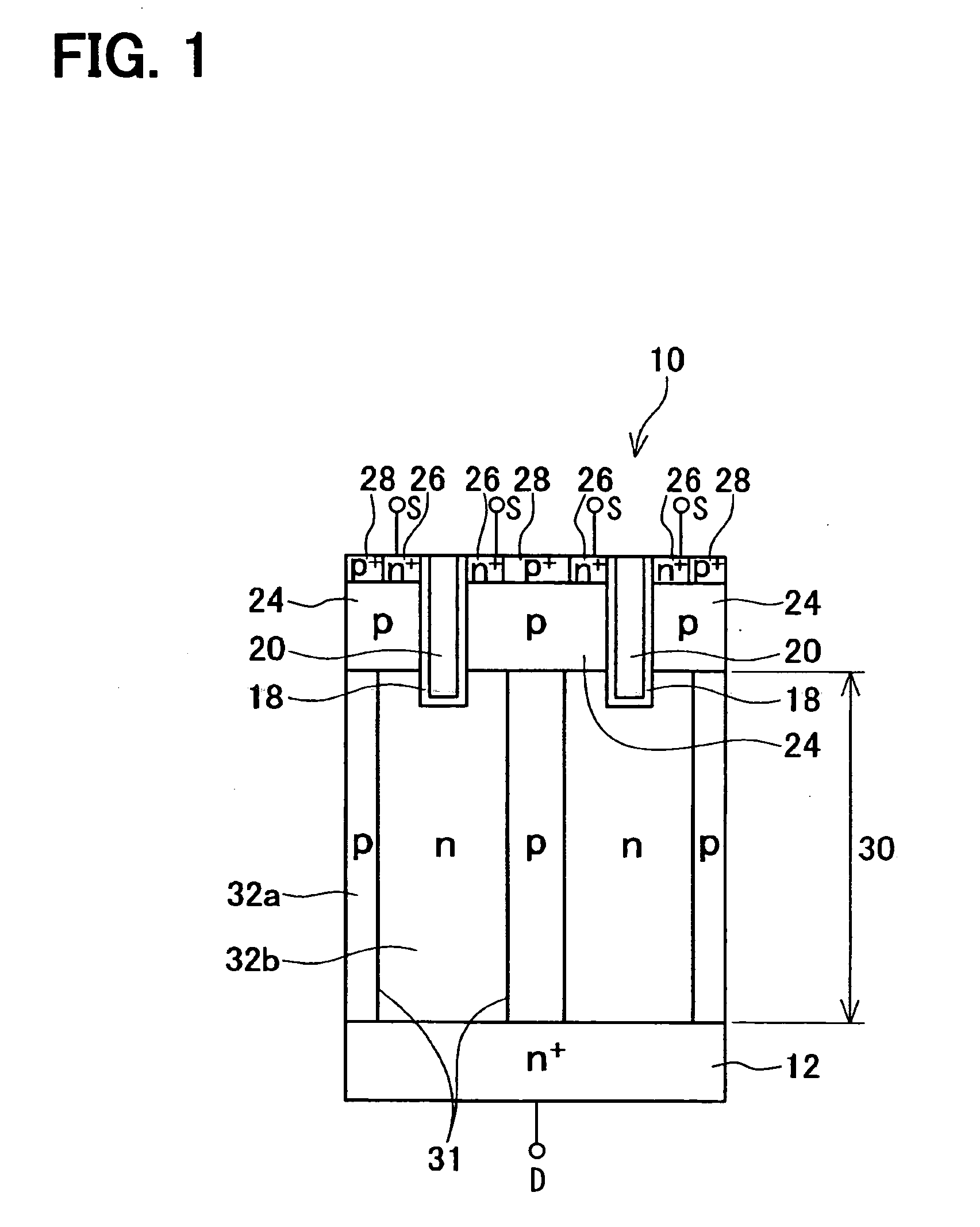
[0024] The inventors have studied about a super junction structure and an on-state resistance changeable in accordance with temperature. Firstly, a MOSFET having a super junction structure has been studied. In FIG. 4 the MOSFET 110 according to a related art includes a N+ conductive type drain layer 112 and a drift layer 132. The drift layer 132 is disposed on a surface of the drain layer 112. A P conductive type body layer 124 is formed on a surface of the drift layer 132. A N+ conductive type source region 126 and a P+ conductive body-contact region 128 are formed on a surface of the body layer 124. The body layer 124 separates the source region 126 from the drift layer 132. A trench gate electrode 120 is formed to penetrate the body layer 124. The trench gate electrode 120 is electrically isolated from the body layer 124 with an insulation film 118.

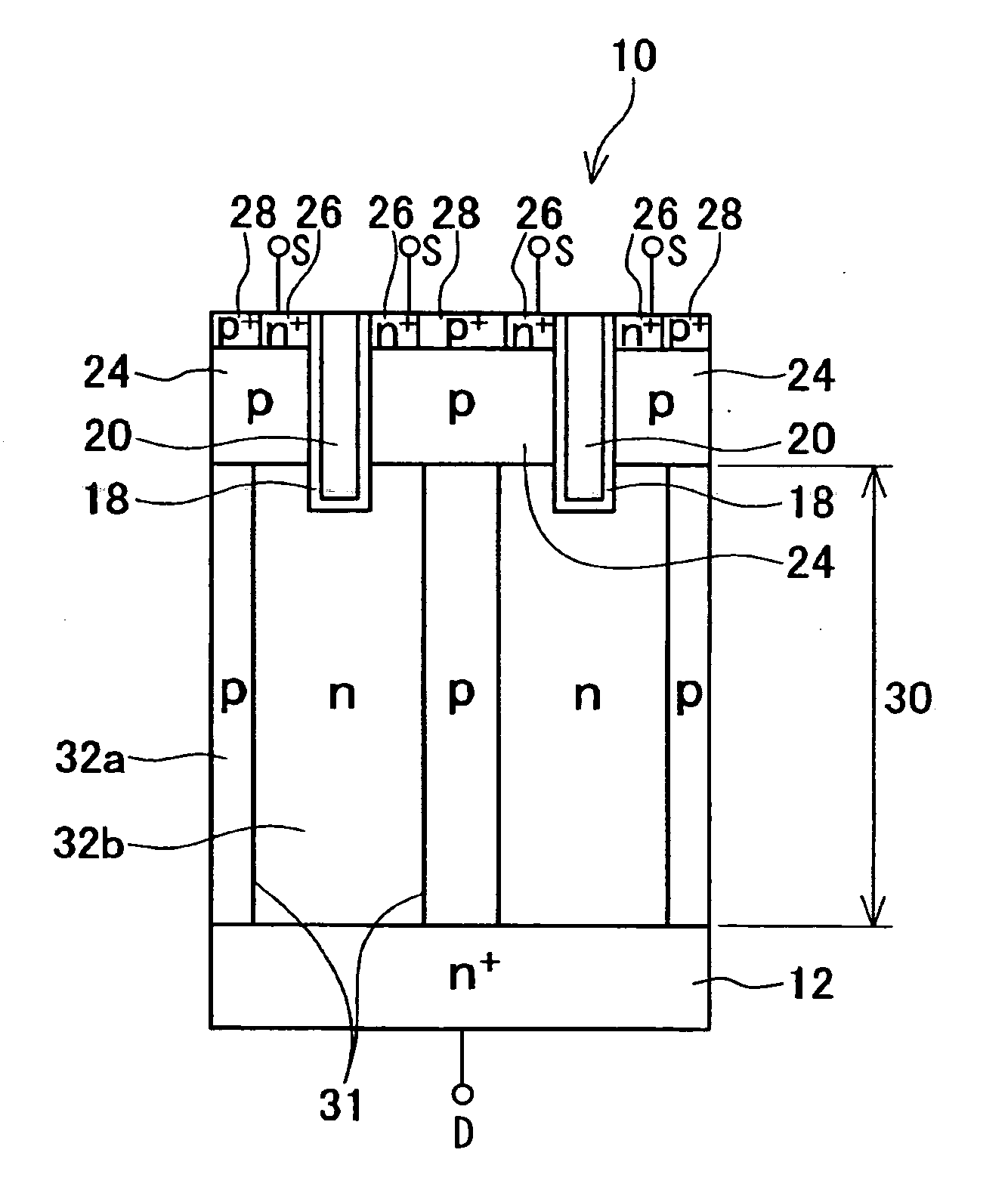
[0025] In FIG. 1, a MOSFET 10 having a super junction structure 30 includes multiple P conductive type columns 32a and N conductive ...


PUM


Abstract

A semiconductor device includes: two main electrodes; multiple first regions; and multiple second regions. The first region having a first impurity concentration and a first width and the second region having a second impurity concentration and a second width are alternately repeated. A product of the first impurity concentration and the first width is equal to a product of the second impurity concentration and the second width. The first width is equal to or smaller than 4.5 μm. The first impurity concentration is lower than a predetermined concentration satisfying a RESURF condition. A ratio between on-state resistances of the device at 27° C. and at 150° C. is smaller than 1.8.

Description

CROSS REFERENCE TO RELATED APPLICATION [0001] This application is based on Japanese Patent Application No. 2005-374170 filed on Dec. 27, 2005, the disclosure of which is incorporated herein by reference. FIELD OF THE INVENTION [0002] The present invention relates to a semiconductor device having a super junction structure. BACKGROUND OF THE INVENTION [0003] To increase a breakdown voltage, a semiconductor device having a region (i.e., a drift region) including a low impurity concentration is disclosed. [0004] By using the drift region, the breakdown voltage of the device is increased. However, an on-state resistance of the device is also increased. Accordingly, it is required to increase the breakdown voltage together with reducing the on-state resistance. In view of this requirement, a super junction structure is proposed. The super junction structure has a first region including a first conductive type impurity and a second region including a second conductive type impurity. The f...

Claims


Application Information

Patent Timeline
IPC IPC(8): H01L29/76
CPCH01L29/0634H01L29/0878H01L29/1095H01L29/36H01L29/7813
Inventor YAMAUCHI, SHOICHIYAMAGUCHI, HITOSHIHATTORI, YOSHIYUKIOKADA, KYOKO
Owner DENSO CORP
Why Eureka
Try Eureka