Semiconductor device
A semiconductor and component technology, applied in the field of semiconductor components, can solve the problem of sacrificing on-state resistance, etc., achieve high breakdown voltage, low on-state resistance, and improve the effect of breakdown voltage
- Summary
- Abstract
- Description
- Claims
- Application Information
AI Technical Summary
Problems solved by technology
Method used
Image

Examples
Embodiment Construction
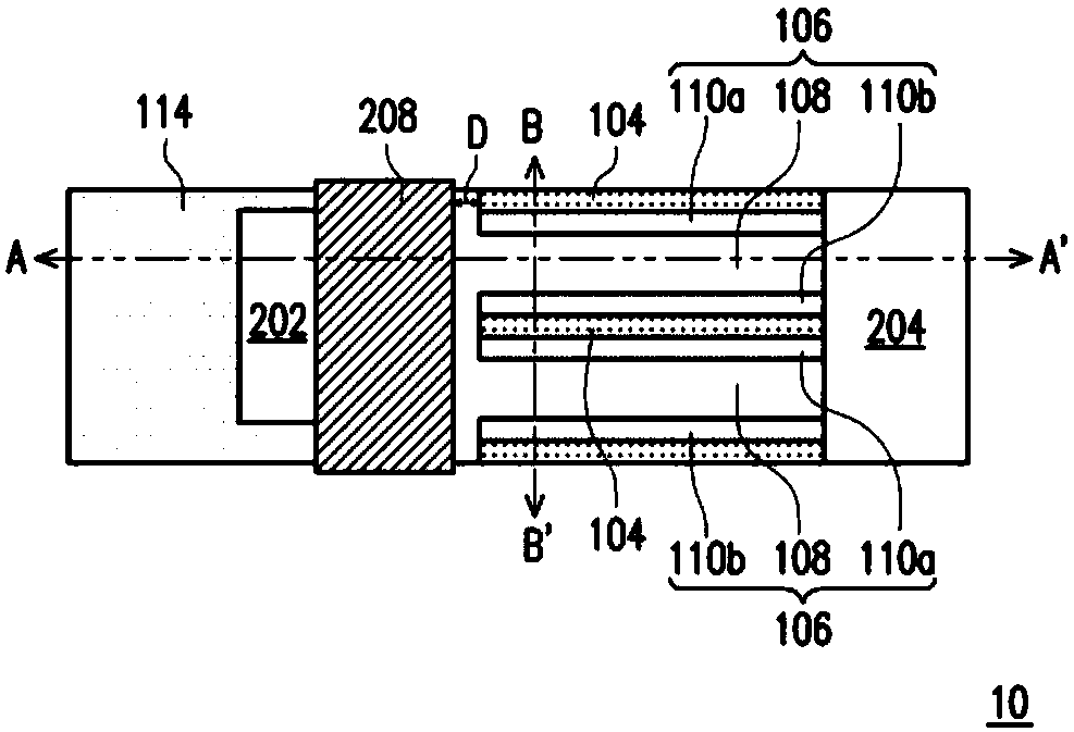
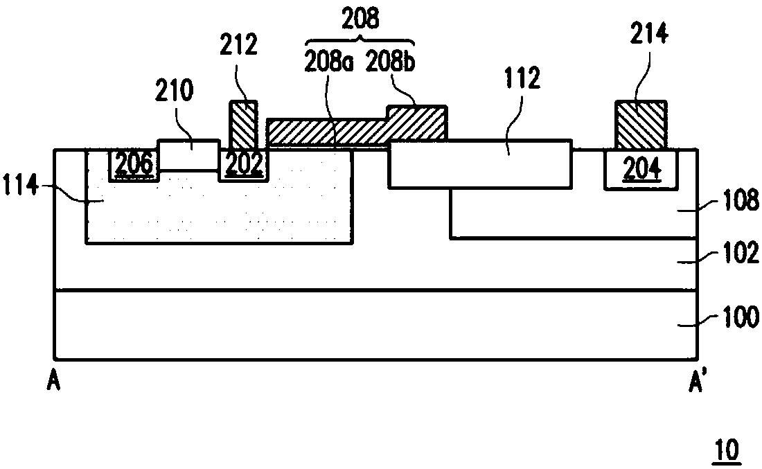
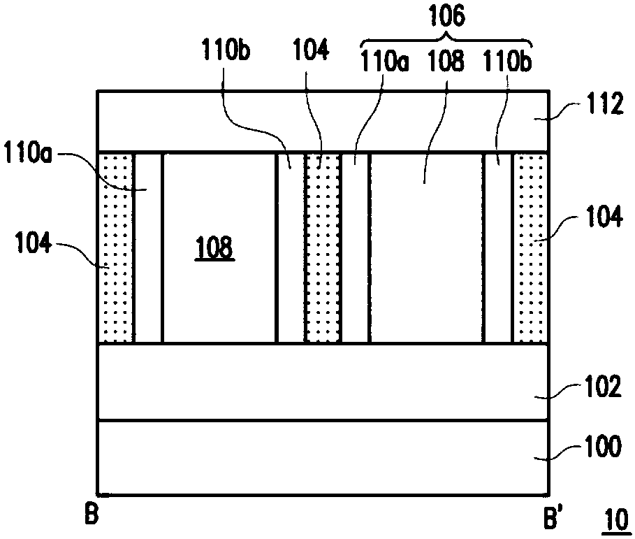
[0033] The present invention will be described more fully with reference to the drawings of the present embodiment. However, the present invention can also be embodied in various forms and should not be limited to the embodiments described herein. The thicknesses of layers and regions in the drawings may be exaggerated for clarity. The same or similar symbols represent the same or similar elements, and the following paragraphs will not repeat them one by one.
[0034] In the following embodiments, the first conductivity type is different from the second conductivity type. In one embodiment, the first conductivity type is N type, and the second conductivity type is P type. In another embodiment, the first conductivity type is P-type, and the second conductivity type is N-type. The P-type dopant is, for example, boron; the N-type dopant, for example, is phosphorus or arsenic. In this embodiment, the first conductivity type is P-type and the second conductivity type is N-type...
PUM
 Abstract
Description
Claims
Application Information
 - Generate Ideas
- Intellectual Property
- Life Sciences
- Materials
- Tech Scout
- Unparalleled Data Quality
- Higher Quality Content
- 60% Fewer Hallucinations
Browse by: Latest US Patents, China's latest patents, Technical Efficacy Thesaurus, Application Domain, Technology Topic, Popular Technical Reports.
© 2025 PatSnap. All rights reserved.Legal|Privacy policy|Modern Slavery Act Transparency Statement|Sitemap|About US| Contact US: help@patsnap.com