Semiconductor assembly and manufacturing method thereof
A manufacturing method, semiconductor technology, applied in the field of its combination and its manufacture, insulated gate bipolar transistor components, can solve problems such as chip bending and deformation
- Summary
- Abstract
- Description
- Claims
- Application Information
AI Technical Summary
Problems solved by technology
Method used
Image

Examples
Embodiment Construction
[0082] In order to further explain the technical means and effects of the present invention to achieve the intended purpose of the invention, the specific implementation, structure, characteristics and methods of the semiconductor component and its manufacturing method proposed according to the present invention will be described below in conjunction with the accompanying drawings and preferred embodiments. Its effect is described in detail below.
[0083] The aforementioned and other technical contents, features and effects of the present invention will be clearly presented in the following detailed description of preferred embodiments with reference to the drawings. For convenience of description, in the following embodiments, the same elements are denoted by the same numbers.
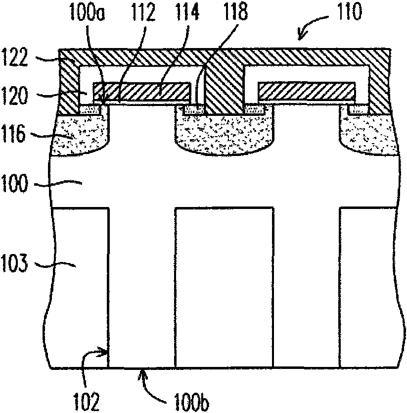
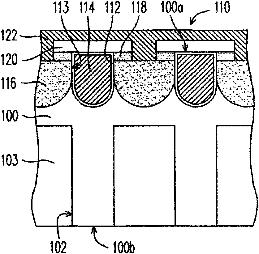
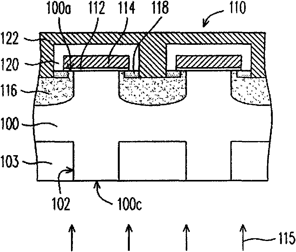
[0084] Figure 1D and Figure 1D-1 They are respectively schematic cross-sectional views of a planar field effect transistor and a trench field effect transistor according to an embodiment of the p...
PUM
 Abstract
Description
Claims
Application Information
 - Generate Ideas
- Intellectual Property
- Life Sciences
- Materials
- Tech Scout
- Unparalleled Data Quality
- Higher Quality Content
- 60% Fewer Hallucinations
Browse by: Latest US Patents, China's latest patents, Technical Efficacy Thesaurus, Application Domain, Technology Topic, Popular Technical Reports.
© 2025 PatSnap. All rights reserved.Legal|Privacy policy|Modern Slavery Act Transparency Statement|Sitemap|About US| Contact US: help@patsnap.com