Protection circuit device using MOSFETs and a method of manufacturing the same
- Summary
- Abstract
- Description
- Claims
- Application Information
AI Technical Summary
Benefits of technology
Problems solved by technology
Method used
Image

Examples
Embodiment Construction
[0045] The mode for carrying out the invention is described referring to FIG. 1 to FIG. 19.
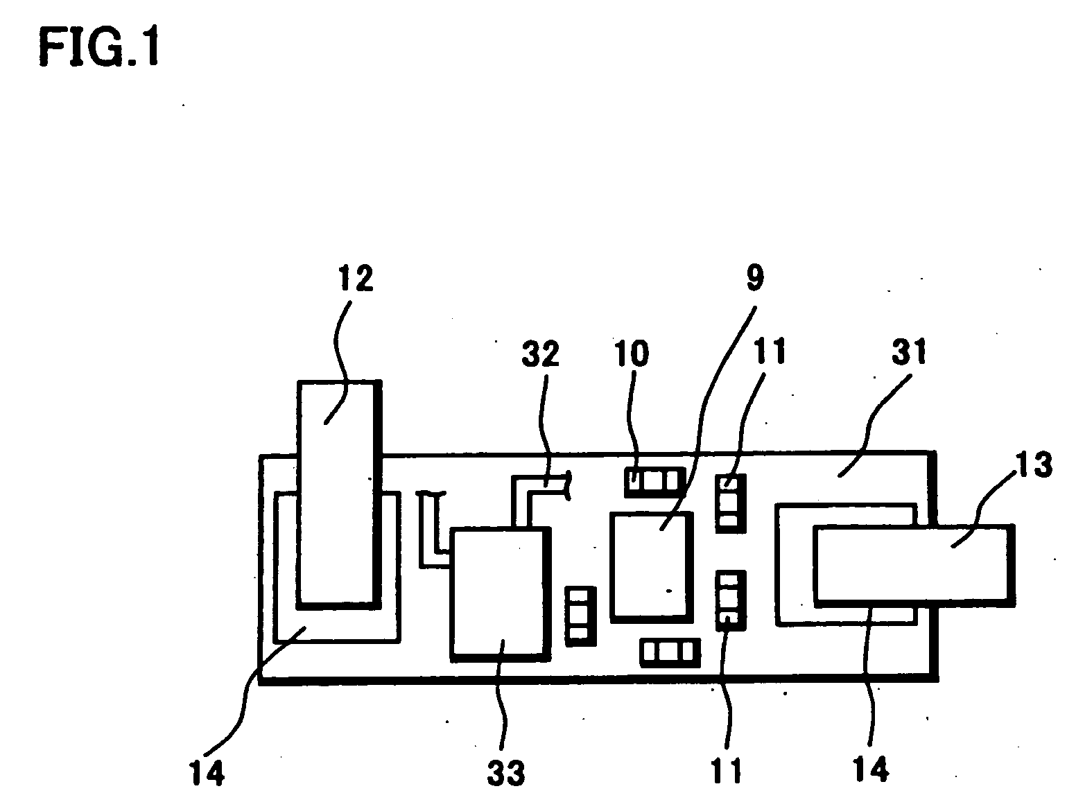
[0046]FIG. 1 shows a plan view of a protection circuit device using the invention. Although circuit parts are mounted as the circuit shown in FIG. 19 is realized in the protection circuit device, the parts are not shown all in the figure. A conductive path 32 comprising copper foil is formed on both face of an insulating board 31, and has multilayer interconnection where the conductive paths 32 of upper face and lower face of the board are connected through through-hole (not shown) at desired position.
[0047] Characteristic of the invention is to mount a MOSFET chip 33 integrating power MOSFETs Q1 and Q2 of switching element in one chip with just bare chip by flip chip method.
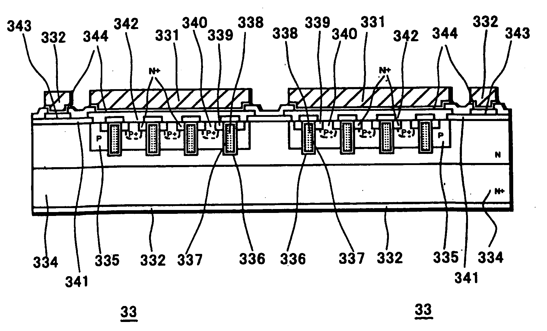
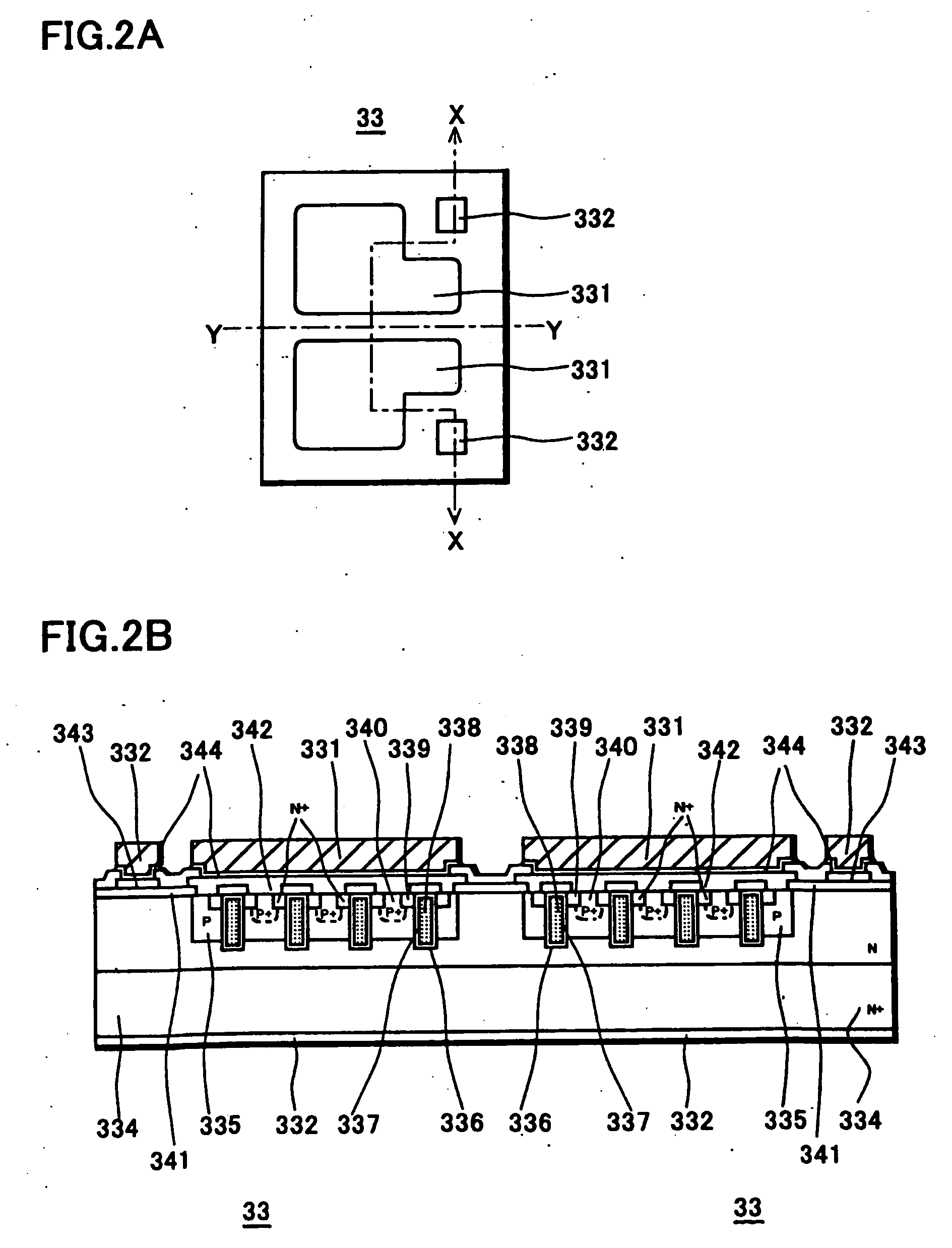
[0048] A structure of concrete structure of the MOSFET chip 33 is shown in FIG. 33. FIG. 2A is a plan view, and FIG. 2B is a section view cut by X-X line.
[0049] The MOSFET chip 33 has an N+ / N semiconductor substrate 33...
PUM
 Abstract
Description
Claims
Application Information
 - Generate Ideas
- Intellectual Property
- Life Sciences
- Materials
- Tech Scout
- Unparalleled Data Quality
- Higher Quality Content
- 60% Fewer Hallucinations
Browse by: Latest US Patents, China's latest patents, Technical Efficacy Thesaurus, Application Domain, Technology Topic, Popular Technical Reports.
© 2025 PatSnap. All rights reserved.Legal|Privacy policy|Modern Slavery Act Transparency Statement|Sitemap|About US| Contact US: help@patsnap.com