IC card with improved plated module

a technology of integrated circuit chips and modules, applied in the field of ic cards, can solve problems such as failure of communication between the integrated circuit chip b>3/b> and the external read-write device b>4/b>, damage to the ck, and failure to disclose the protection of such an integrated circuit chip, so as to reduce the effect of these forces

Inactive Publication Date: 2007-07-05
STMICROELECTRONICS INT NV
View PDF8 Cites 203 Cited by
  • Summary
  • Abstract
  • Description
  • Claims
  • Application Information

AI Technical Summary

Benefits of technology

[0011] The aim of the present invention is to provide an IC card resistant to forces due to bending or deforming the plastic support of the IC card, especially reducing the effect of these forces in proximity to the recess of the plastic support in which the printed circuit and the integrated circuit chip are inserted and fixed.
[0012] Another aim of the present invention is to provide an IC card resistant to possible breakage of portions of conductive areas or their partial detachment from the recess, in order to preserve the use of the IC card also when such breaks or partial detachment occur.
[0013] A further aim of the present invention is to safeguard the contact points between the conductive areas and the integrated circuit and to reinforce the connection between the pads and the antenna.

Problems solved by technology

. . ck may be damaged, causing the communication between the integrated circuit chip 3 and the external read write device 4 to fail.
Even if the bypass stress is intended to protect the integrated circuit chip from forces, it does not disclose how to protect such an integrated circuit chip when it is connected to an antenna, for example when the IC card is a combined IC card.
Such mechanical discontinuity is provided outside the area wherein the integrated circuit chip and the antenna are positioned, resulting in a substantial modification of the plated or protective module that supports the antenna and the integrated circuit chip.

Method used


Image

  • IC card with improved plated module
  • IC card with improved plated module
  • IC card with improved plated module

Examples


Embodiment Construction

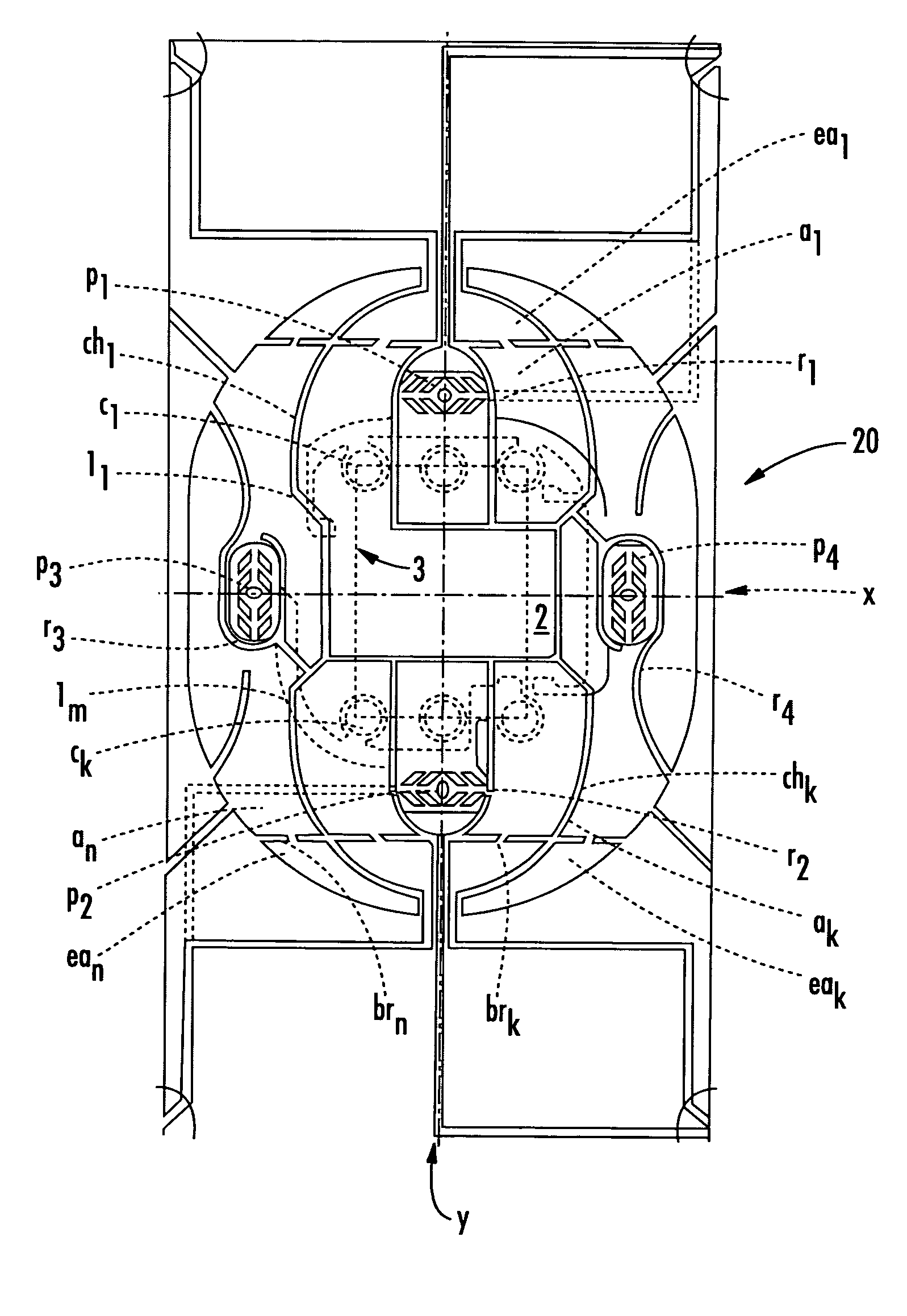
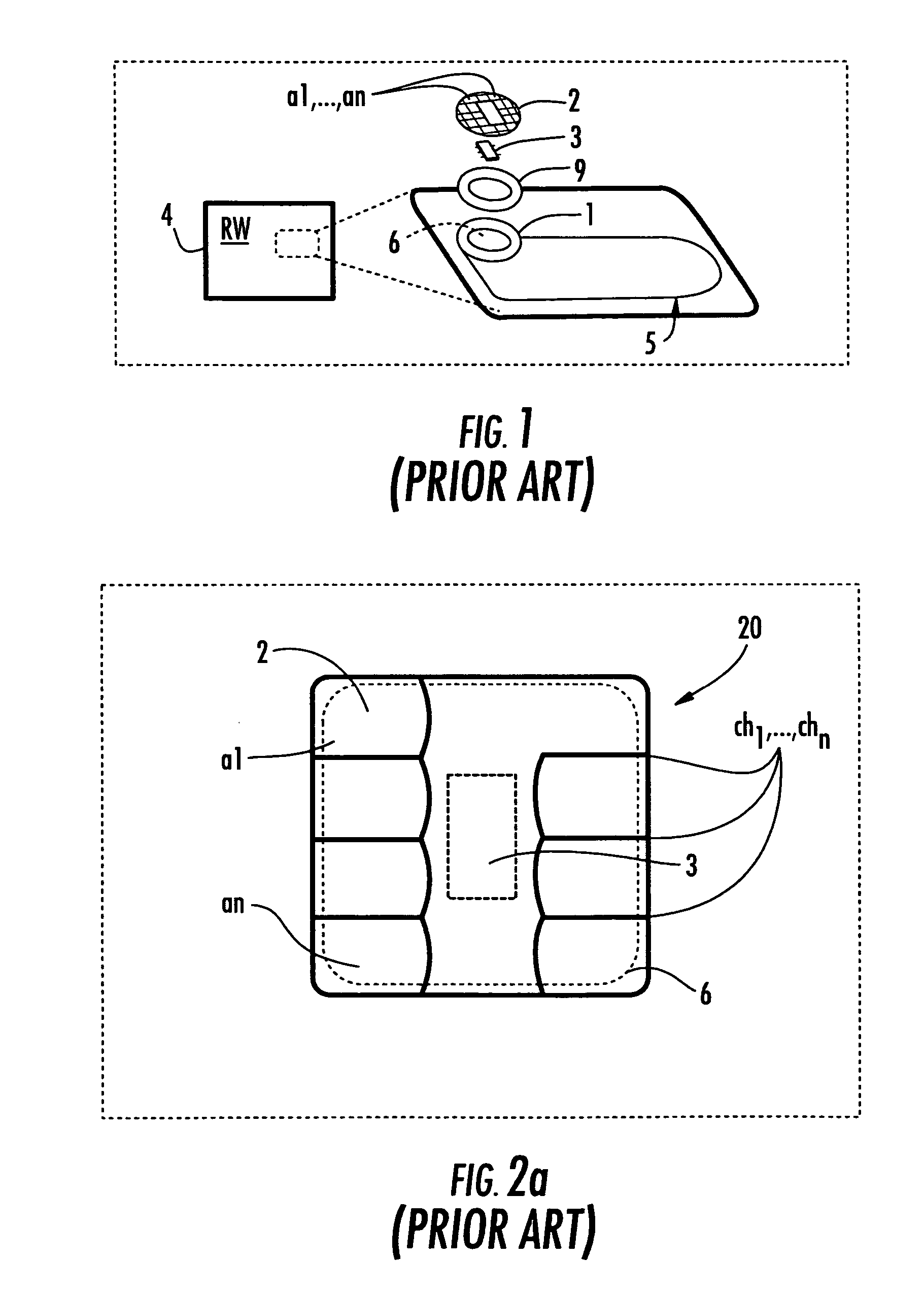
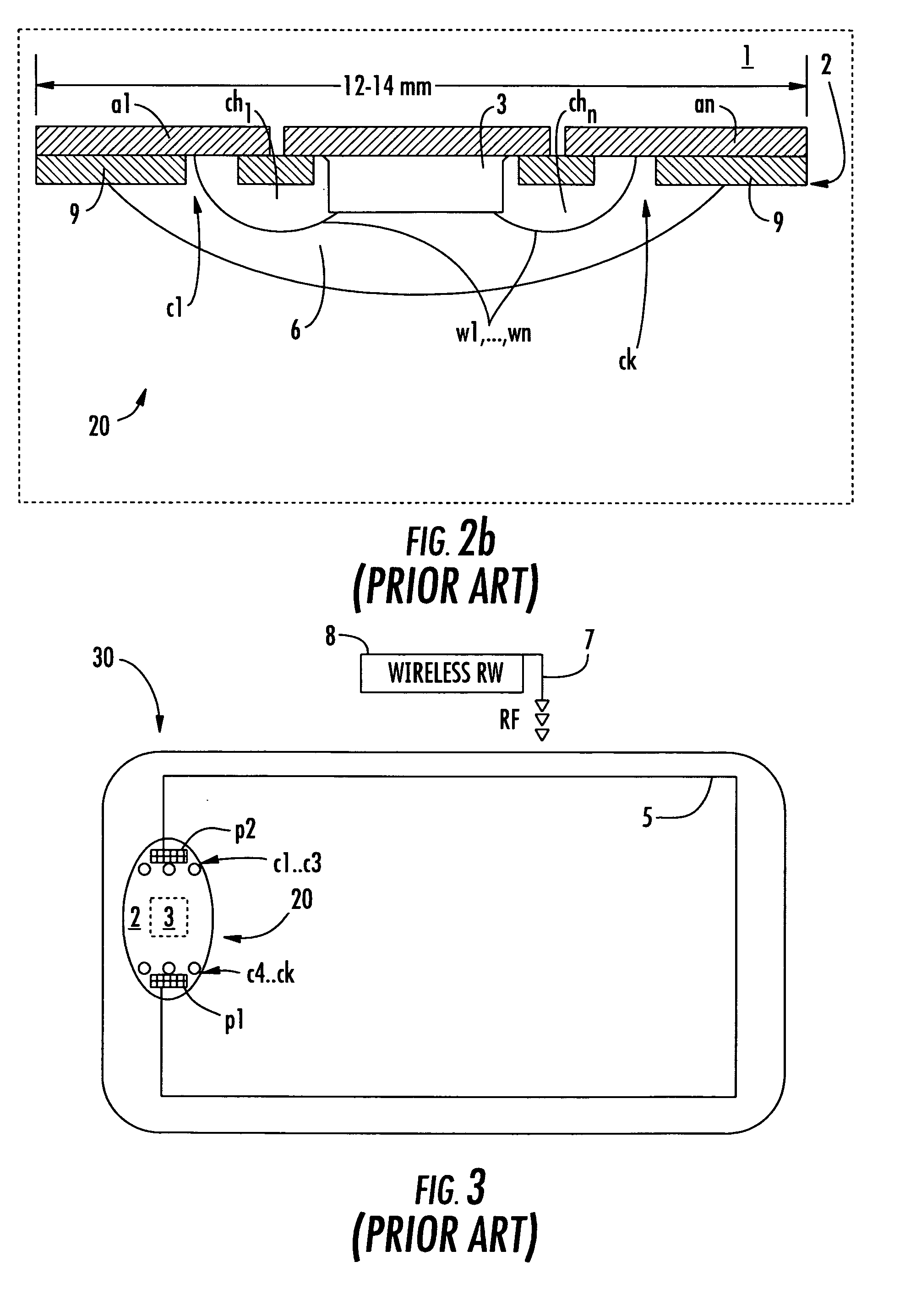
[0024] With reference to FIG. 4 is shown and is globally indicated with 30 an IC card comprising a plastic support 1 and a plated module 20, glued inside a recess 6 not explicitly shown because conventional. The plated or protective module 20 includes a printed circuit 2, comprising a plurality of conductive areas a1, . . . , an, delimited by a network of insulating channels ch1, . . . , chn, covering an integrated circuit chip 3.

[0025] More particularly, as shown in FIG. 5, at least some of the conductive areas a1, . . . , an are connected through wire bonding w1, . . . , wk to a corresponding contact point c1, . . . , ck on the integrated circuit chip 3, so as to provided communication connection between an external read write device 4 and the integrated circuit chip 3. Accordingly, a plurality extended areas ea1, . . . , eam at the border of the recess 6 are linked to at least some of the conductive areas a1, . . . , an through one or more bridge br1, . . . , brn.

[0026] An exte...


PUM


Abstract

An IC card includes a plated or protective module including a printed circuit having a plurality of conductive areas, delimited by a network of insulating channels, for covering an integrated circuit chip, a plastic support with a recess intended to host the plated module and the integrated circuit chip, with at least some of the conductive areas connected to corresponding contact points on the integrated circuit chip. A plurality of extended areas are linked to a corresponding conductive areas by one or more bridges. A couple of advanced extended areas form a rounded border of the plated module. Advanced extended areas are linked to conductive areas not connected to contact points. Advanced extended areas wrap around the extended areas and form the opposite rounded sides of the plated module.

Description

FIELD OF THE INVENTION [0001] The present invention relates to an IC card comprising a plastic support with a recess, an integrated circuit chip hosted in the recess, a plated module including a printed circuit comprising a plurality of conductive areas, delimited by a network of insulating channels, for covering the integrated circuit chip, with at least some of the conductive areas being connected to a corresponding contact point of the integrated circuit chip. BACKGROUND OF THE INVENTION [0002] As is well known an IC card generally comprises a plastic support with a recess, an integrated circuit chip and a printed circuit, with the printed circuit wire bonded on the integrated circuit chip and glued inside the recess with an epoxy resin. With reference to FIG. 1, an IC card 10 is represented in an exploded view, with the plastic support indicated with numeral reference 1, the recess with 6, the printed circuit and the integrated circuit chip respectively indicated with numeral re...

Claims


Application Information

Patent Timeline
Patent Type & Authority Applications(United States)
IPC IPC(8): G06K19/06
CPCG06K19/07743G06K19/07745G06K19/0775G06K19/07769H01L2224/48228H01L2224/48091H01L2924/00014
Inventor FRALLICCIARDI, PAOLOVISCONTI, EDOARDO
Owner STMICROELECTRONICS INT NV
Why Eureka
Try Eureka