Active component array substrate

a technology of active components and array substrates, which is applied in the direction of instruments, semiconductor devices, electrical apparatus, etc., can solve the problems of increasing the length of metal wires within liquid crystal displays, not meeting the market trend of being light, thin, chic, and low power consumption, and reducing the impedance difference between wires.

Inactive Publication Date: 2007-07-05
AU OPTRONICS CORP
View PDF2 Cites 5 Cited by
  • Summary
  • Abstract
  • Description
  • Claims
  • Application Information

AI Technical Summary

Benefits of technology

[0009]In view of the above, an object of the present invention is to provide an active component array substrate for reducing the impedance difference among wires in the non-display region.
[0022]According to the above, the present invention utilizes multiple parallel-connected conductor layers as part of or all of the wires in the non-display region. Therefore, compared with the conventional technique where the wires all employ a single conductor layer, the present invention is able to reduce the impedance difference between wires, so that non-uniform image displaying is improved.

Problems solved by technology

However, with the prevalence of the concept of “green” environmental protection, due to the properties of large power consumption and radiation, as well as limited flat space for the product, the CRT may not satisfy the market trend for being light, thin, short, small, chic, and low in power consumption.
However, as the size of current liquid crystal displays has gradually become increasingly large, the length of metal wires within liquid crystal displays is also gradually increased, such that the impedance increase of the metal wires and the signal delay are more and more acute.

Method used


Image

  • Active component array substrate
  • Active component array substrate
  • Active component array substrate

Examples


first embodiment

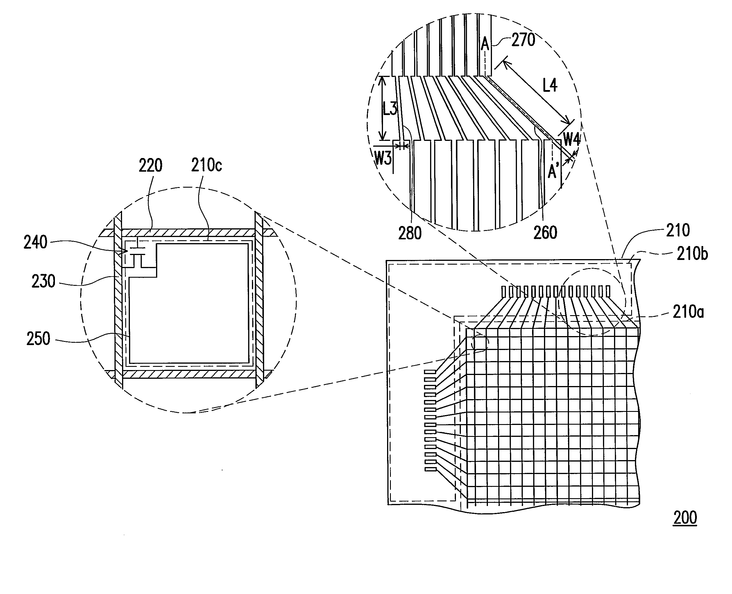
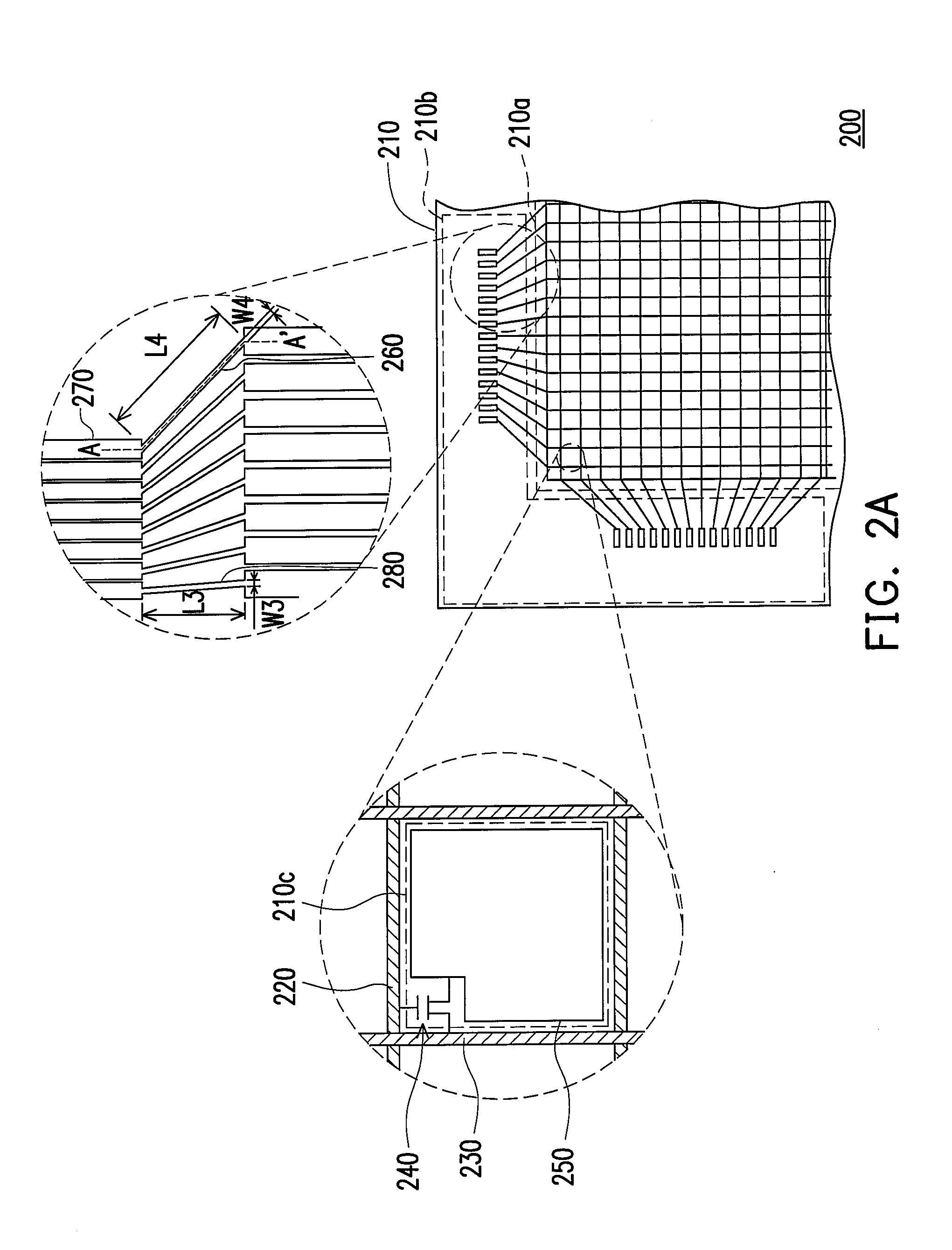
[0030]FIG. 2A illustrates a top view of an active component array substrate according to the first preferred embodiment of the present invention, and FIG. 2B illustrates a cross-sectional view along the A-A′ line of FIG. 2A. Referring to FIGS. 2A and 2B, the active component array substrate 200 of this embodiment includes a substrate 210, a plurality of scan lines 220, a plurality of data lines 230, a plurality of switch components 240, a plurality of pixel electrodes 250, a plurality of first wires 260, a plurality of second wires 280, and a plurality of pads 270, wherein the substrate 210 includes a display region 210a and a non-display region 210b. Moreover, the scan lines 220 and data lines 230 are disposed in the display region 210a. The scan lines 220 and the data lines 230 divide the display region 210a into a plurality of the pixel regions 210c. Further, the switch components 240 are respectively disposed in the pixel regions 210c, and are controlled by the scan lines 220 an...

second embodiment

[0038]FIGS. 3A to 3E illustrate cross-sectional views of the first wires according to the second preferred embodiment of the present invention. Referring to FIG. 3A first, FIG. 3A is similar to FIG. 2B, with the only difference lying in that: to further reduce the impedance, the first wire 260 further includes a third conductor layer 262c disposed on the second conductor layer 262b. The first conductor layer 262a, the second conductor layer 262b, and the third conductor layer 262c are electrically parallel-connected. In this embodiment, the first conductor layer 262a and the scan lines 220 may be in the same layer; the second conductor layer 262b and the data lines 230 may be in the same layer; and the third conductor layer 262c and the pixel electrodes 250 may be in the same layer.

[0039]Referring to FIG. 3B, FIG. 3B is similar to FIG. 2C, with the only difference lying in that: after the second conductor layer 262b is formed, the third conductor layer 262c is formed on the second c...


PUM


Abstract

Scan lines and data lines are disposed in a display region of a substrate, and multiple pixel regions are divided thereon. Switch components are disposed in the pixel regions, and each switch component is electrically connected to the scan line and data line. Pixel electrodes are disposed in the pixel regions and each pixel electrode is electrically connected to the switch component. Wires are disposed in a non-display region of the substrate, and at least one portion of each wire includes a first and a second conductor layer, wherein the second conductor layer is disposed on the first conductor layer and parallel-connected to the first conductor layer. The first conductor layer and one of the scan lines, data lines, and the pixel electrodes are in the same layer. The second conductor layer and another one of the scan lines, data lines, and the pixel electrodes are in the same layer.

Description

CROSS-REFERENCE TO RELATED APPLICATION[0001]This application claims the priority benefit of Taiwan application serial no. 94147534, filed on Dec. 30, 2005. All disclosure of the Taiwan application is incorporated herein by reference.BACKGROUND OF THE INVENTION[0002]1. Field of Invention[0003]The present invention relates to a component array substrate, more particularly, to an active component array substrate.[0004]2. Description of Related Art[0005]With the continuously increasing demand for displays, the manufacturers in the field exert their efforts to the development of relative displays. Among all kinds of displays, the cathode ray tube (CRT) has ranked first in the display market due to its excellent display quality and mature technology. However, with the prevalence of the concept of “green” environmental protection, due to the properties of large power consumption and radiation, as well as limited flat space for the product, the CRT may not satisfy the market trend for being...

Claims


Application Information

Patent Timeline
Patent Type & Authority Applications(United States)
IPC IPC(8): H01L29/04
CPCG02F1/136286H01L27/124G02F2001/13629G02F1/13629G02F1/136
Inventor HUNG, MENG-YI
Owner AU OPTRONICS CORP
Why Eureka
Try Eureka