Electrophotographic photosensitive member and image forming apparatus provided with the same

a photosensitive member and electrophotography technology, applied in the direction of electrographic process apparatus, instruments, corona discharge, etc., can solve the problems of defective image formation on recording media, similar problems

Active Publication Date: 2007-07-05
KYOCERA CORP
View PDF4 Cites 15 Cited by
  • Summary
  • Abstract
  • Description
  • Claims
  • Application Information

AI Technical Summary

Benefits of technology

[0014] An object of the present invention is to prevent a photosensitive layer of electrophotographic photosensitive member from being broken at side of a power transmission flange, so that no defective image is formed.

Problems solved by technology

If the photoconductive layer of the photosensitive layer is broken and the crack extends to the cylindrical body, electrification charge originally existing on the surface of the photosensitive member moves to the cylindrical body through the crack (providing electrical short circuit), thereby forming a defective image on a recording medium.
Specifically, even when a bearing flange (without a shaft) is firmly fixed to the electrophotographic photosensitive member and a shaft is inserted into a through-hole formed at the bearing flange via a bearing, problem similar to the above-described one may be caused due to a slight play at the bearing.

Method used


Image

  • Electrophotographic photosensitive member and image forming apparatus provided with the same
  • Electrophotographic photosensitive member and image forming apparatus provided with the same
  • Electrophotographic photosensitive member and image forming apparatus provided with the same

Examples


example 1

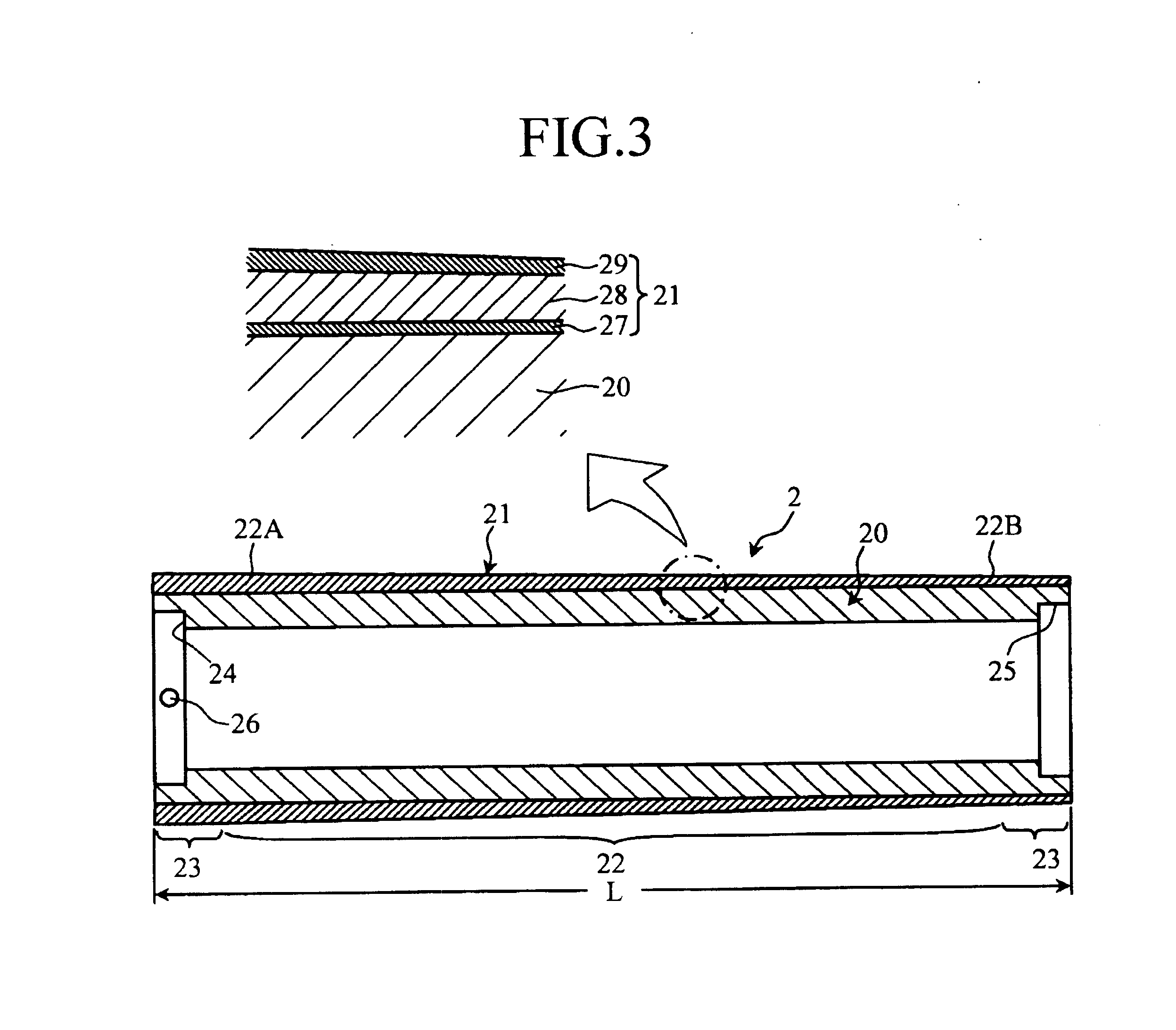
[0095] In the present example, influence on the image property was studied, when changing the thickness at the ends of the surface layer of the electrophotographic photosensitive member.

[0096] (Manufacture of Electrophotographic Photosensitive Member)

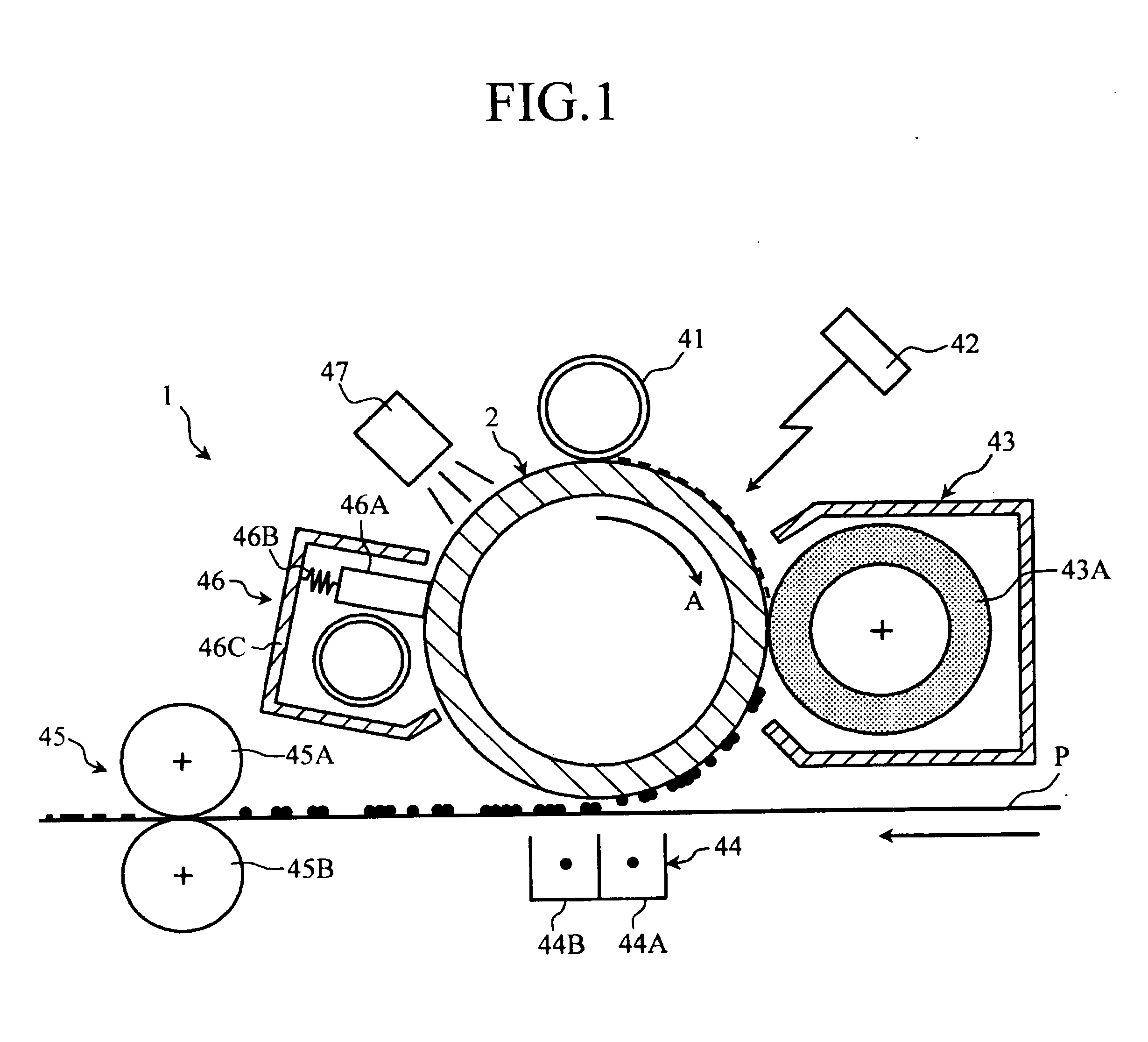
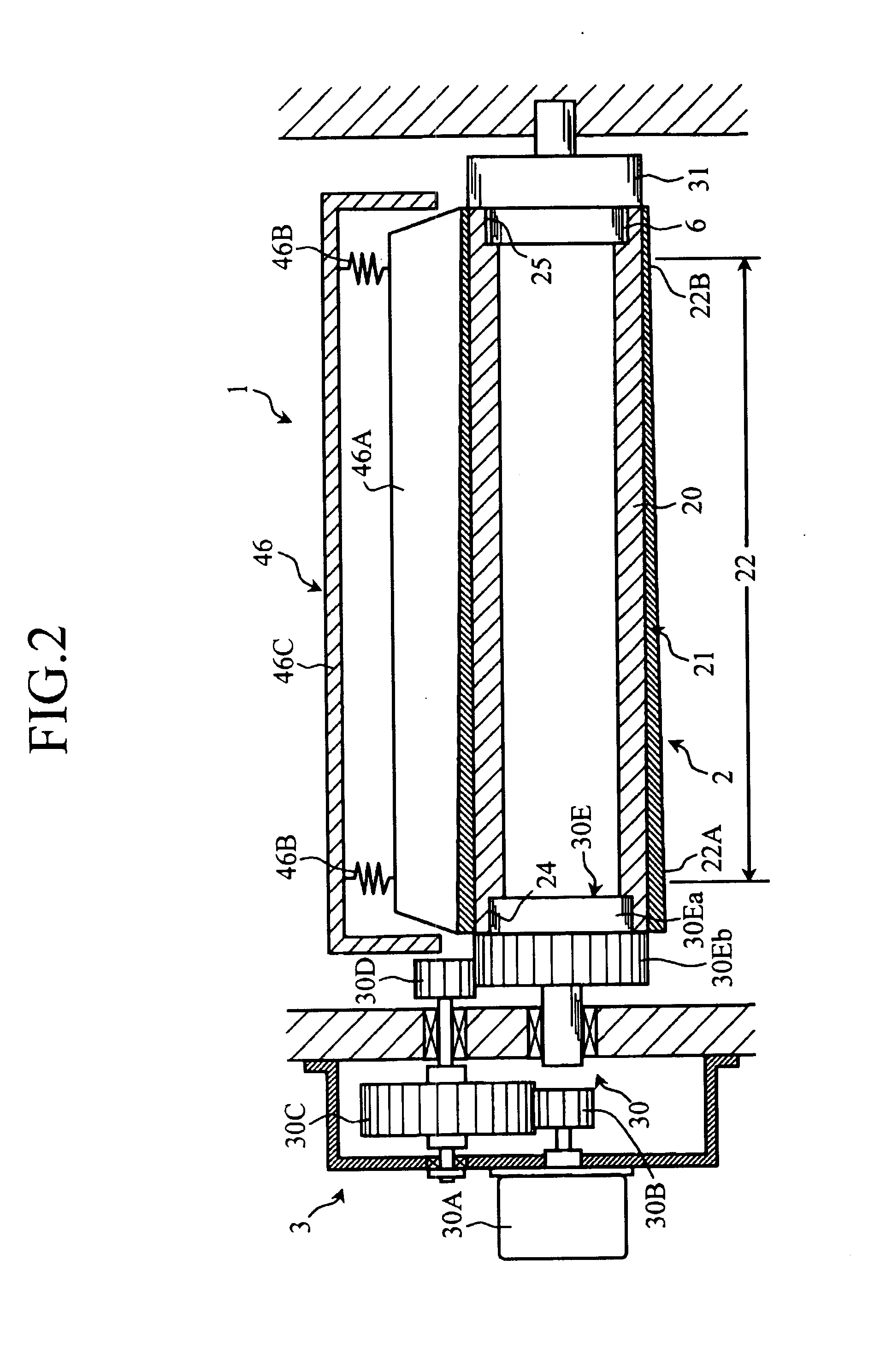
[0097] In manufacturing the electrophotographic photosensitive member, a cylindrical body was prepared by making a drawn tube of aluminum alloy with outer diameter of 84 mm and length of 360 mm, and then performing mirror finishing on the outer circumference of the drawn tube before cleaning. Next, the prepared cylindrical body 20 was incorporated in the glow discharge decomposition device 5 shown in FIGS. 4 and 5, and an anti-charge injection layer and a photoconductive layer were laminated on the surface of the cylindrical body 20 using a gas inlet tube 55′ shown in FIG. 8 under film forming conditions shown in Table 1. Thereafter, a surface layer was formed on the photoconductive layer using the gas inlet tube 55 shown in FIG. 6 un...

example 2

[0111] In the present example, influence on the image property was studied, when changing the proportion of thickness of the surface layer at the side of the power transmission flange to the thickness at the side of the bearing flange.

[0112] (Manufacture of Electrophotographic Photosensitive Member)

[0113] Electrophotographic photosensitive members C, D, E, F were manufactured by the same method as Example 1. Specifically, an anti-charge injection layer and a photoconductive layer were laminated on the surface of the cylindrical body 20 using the gas inlet tube 55′ shown in FIG. 11 under film forming conditions shown in Table 1. Thereafter, a surface layer was formed on the photoconductive layer using the gas inlet tube 55 shown in FIG. 6 under film forming conditions shown in Table 2.

[0114] The gas inlet tubes 55 for forming the surface layers had respective gas inlet ports arranged differently in the area X (see FIG. 6), so that the surface layers of the electrophotographic phot...

example 3

[0122] In the present example, influence on the image property was studied, when changing the thickness at the ends of the photoconductive layer of the electrophotographic photosensitive member.

[0123] (Manufacture of Electrophotographic Photosensitive Member)

[0124] An electrophotographic photosensitive member G (hereinafter referred to as “photosensitive member G”) was manufactured by the same method as Example 1. Specifically, an anti-charge injection layer was formed on the surface of the cylindrical body 20 using the gas inlet tube 55′ shown in FIG. 11 under film forming conditions shown in Table 1. Next, a photoconductive layer was laminated on the anti-charge injection layer using the gas inlet tube 55 shown in FIG. 6 under film forming conditions shown in Table 1. Thereafter, a surface layer was laminated on the photoconductive layer using the gas inlet tube 55′ again, under film forming conditions shown in Table 2.

[0125] In the gas inlet tube 55 shown in FIG. 6, the gas in...


PUM


Abstract

The present invention relates to an electrophotographic photosensitive member and an image forming apparatus provided with the same. The electrophotographic photosensitive member includes a substantially cylindrical body and a photosensitive layer having a latent image forming area formed on the body. In the photosensitive layer incorporated in the image forming apparatus, a first end in the axial direction of the latent image forming area is pressed harder than a second end at opposite side of located opposite to the first end in the axial direction. In the photosensitive layer, thickness or dynamic indentation hardness at the first end at one side of the latent image forming area is larger than thickness or dynamic indentation hardness at the second end at opposite side of located opposite to the first end in the axial direction of the latent image forming area.

Description

TECHNICAL FIELD [0001] The present invention relates to an electrophotographic photosensitive member and an image forming apparatus provided with the same. BACKGROUND ART [0002] An image forming apparatus such as a copying machine and a printer utilizing electrophotographic method is provided with an electrophotographic photosensitive member. In such image forming apparatus, the electrophotographic photosensitive member is rotated by a power transmitter, and synchronously with the rotation, operations such as electrification, exposure, development, transfer, and cleaning are repeated, thereby forming an image on a recording medium. [0003] Specifically, in the image forming apparatus, the electrophotographic photosensitive member is electrically charged at its surface and then rotated while being irradiated by laser light for exposure, according to an image pattern, so that an electrostatic latent image is formed on the surface of the electrophotographic photosensitive member. Next, ...

Claims


Application Information

Patent Timeline
Patent Type & Authority Applications(United States)
IPC IPC(8): G03G15/00G03G5/14
CPCG03G15/751
Inventor FUKUNAGA, HIDEAKIISHII, YOSHINOBU
Owner KYOCERA CORP
Why Eureka
Try Eureka