Semiconductor device having SOI substrate

a semiconductor and substrate technology, applied in the direction of semiconductor devices, electrical devices, transistors, etc., can solve the problems of variable threshold voltage and leak current in the semiconductor element, and the way to suppress the floating body effect has not been conventionally proposed

Inactive Publication Date: 2007-07-12
KK TOSHIBA
View PDF2 Cites 141 Cited by
  • Summary
  • Abstract
  • Description
  • Claims
  • Application Information

AI Technical Summary

Problems solved by technology

The floating body effect has a problem that variations in the threshold voltage and leak current in the semiconductor element are caused.
However, when the comb structure is applied to the SOI structure, the way how to suppress the floating body effect has not been conventionally proposed.

Method used


Image

  • Semiconductor device having SOI substrate
  • Semiconductor device having SOI substrate
  • Semiconductor device having SOI substrate

Examples


first embodiment

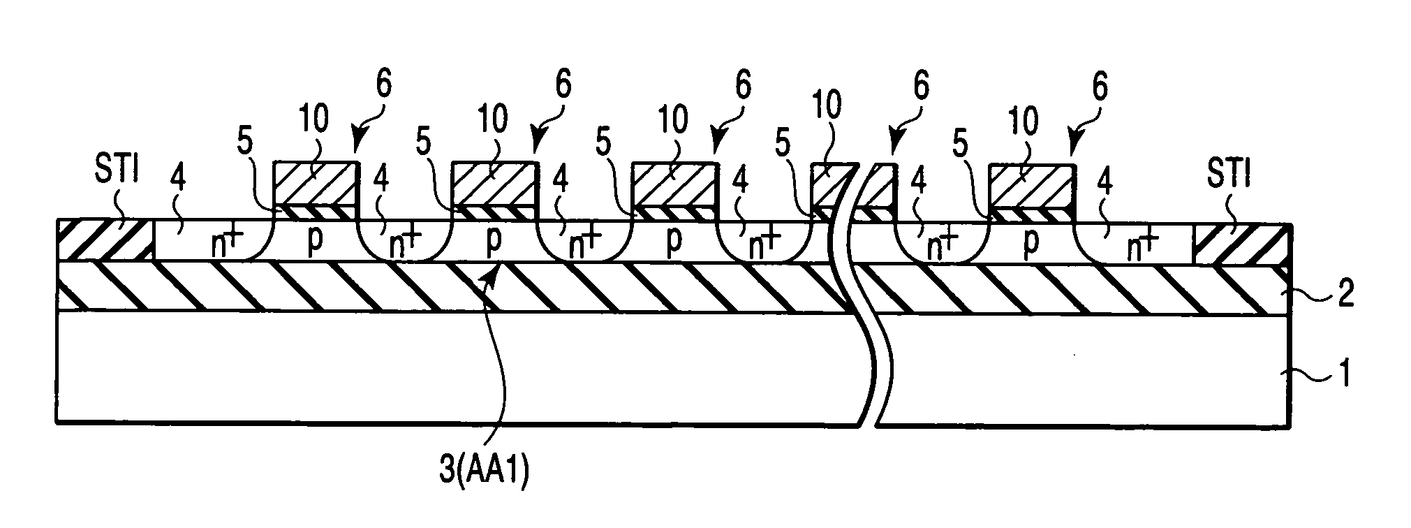
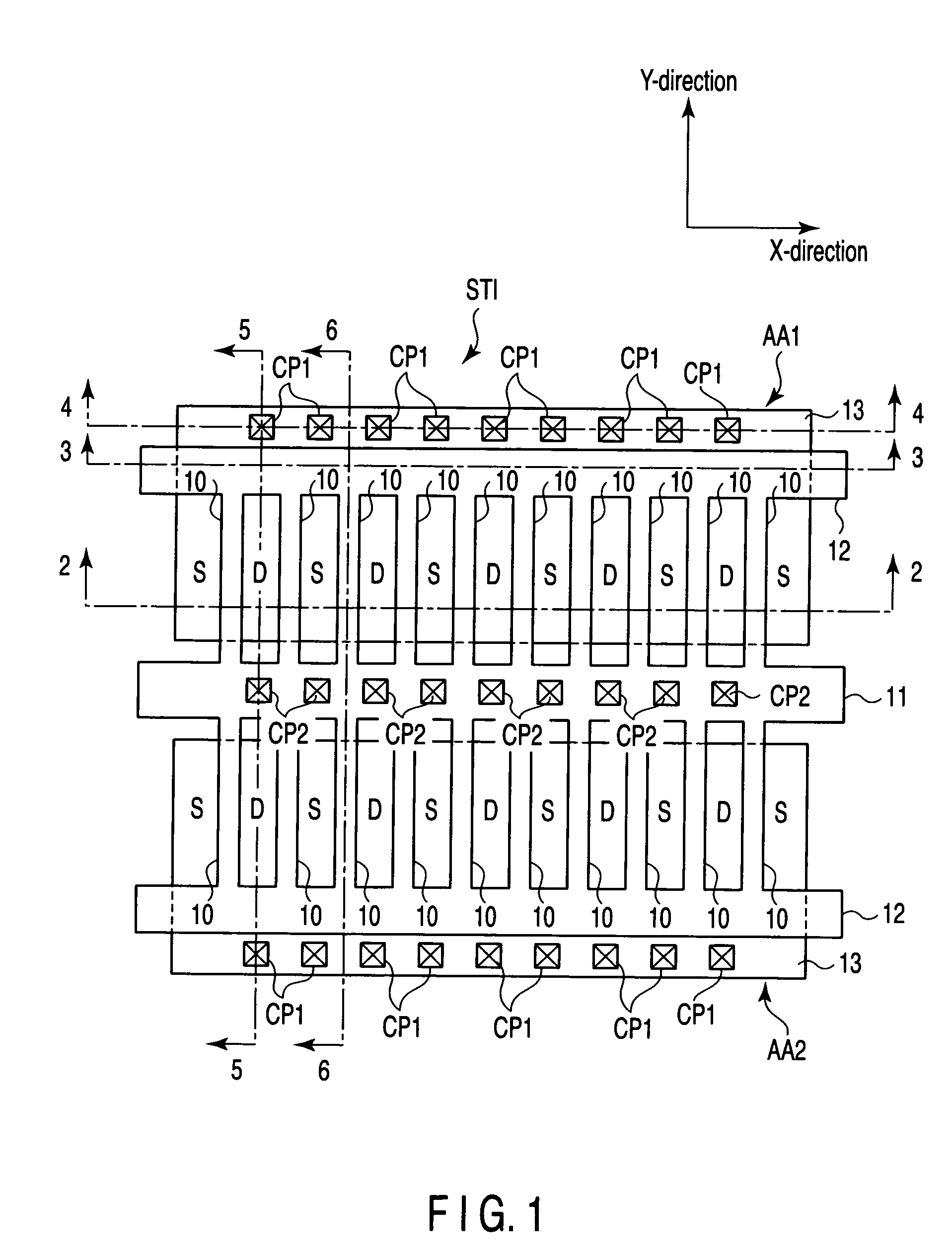
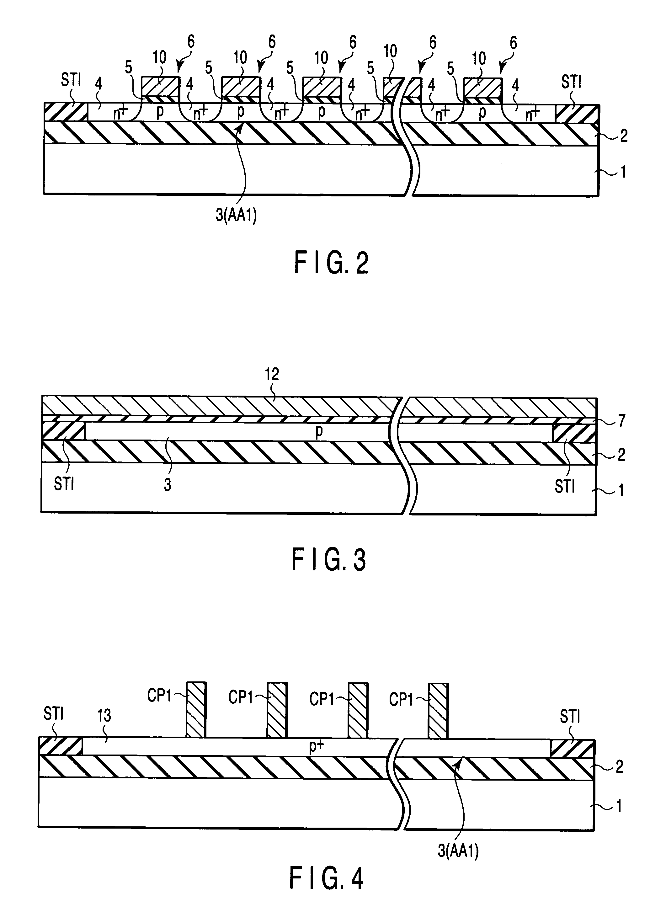
[0061] There will now be described a semiconductor device according to this invention with reference to FIG. 1. FIG. 1 is a plan view of an analog CMOS circuit according to the present embodiment.

[0062] As shown in FIG. 1, the CMOS circuit includes two element regions AA1, AA2. The element regions AA1, AA2 are p-type semiconductor regions formed on an insulating film which is formed on a semiconductor substrate (not shown). The two element regions AA1, AA2 are separated from each other and arranged to extend in a Y direction. The element regions AA1, AA2 are surrounded by an element isolation region STI and the element regions AA1 and AA2 are electrically isolated from each other by the element isolation region STI. A plurality of stripe-shaped gate electrodes 10 are formed to extend in a Y direction on the element regions AA1, AA2 with gate insulating films (not shown) disposed therebetween. The gate electrodes 10 are arranged in an X direction which is perpendicular to the Y direc...

second embodiment

[0102] As shown in FIG. 24, the structure of the present embodiment and the structure of FIG. 7 explained in the second embodiment can be combined. FIG. 24 is a plan view of a CMOS circuit according to a first modification of the present embodiment. As shown in FIG. 24, contact plugs CP4 can be additionally formed on the wiring layers 22 in the structure shown in FIG. 21. Of course, it is possible to further extend the wiring layer 22 in the Y direction in FIG. 24.

[0103] As shown in FIG. 25, the structure according to the present embodiment can be applied to the structure shown in FIG. 20. FIG. 25 is a plan view of a CMOS circuit according to a second modification of the present embodiment. As shown in FIG. 25, wiring layers 24 can be additionally formed in the structure shown in FIG. 20.

[0104] Next, a semiconductor device according to a fourth embodiment of this invention is explained. The present embodiment can be attained by applying the structure explained in the first to third...


PUM


Abstract

A semiconductor device includes first semiconductor layers with a first conductivity, second to fifth semiconductor layers with a second conductivity, gate electrodes, and a first wiring layer. The second semiconductor layers are each disposed between adjacent ones of the first semiconductor layers. The third semiconductor layer is in contact with the second semiconductor layers. The gate electrodes are formed on the second semiconductor layers. The fourth semiconductor layer is in contact with the third semiconductor layer. The first wiring layer is formed on the third semiconductor layer and commonly connects the gate electrodes. The length of the fourth semiconductor layer in the lengthwise direction is smaller than the length of the third semiconductor layer in the lengthwise direction. The fifth semiconductor layer is in contact with the fourth semiconductor layer and isolated from the first semiconductor layers by the fourth semiconductor layer.

Description

CROSS-REFERENCE TO RELATED APPLICATIONS [0001] This application is based upon and claims the benefit of priority from prior Japanese Patent Application No. 2006-005054, filed Jan. 12, 2006, the entire contents of which are incorporated herein by reference. BACKGROUND OF THE INVENTION [0002] 1. Field of the Invention [0003] This invention relates to a semiconductor device and, for example, this invention relates to the structure of MOS transistors formed on an SOI (Silicon On Insulator) substrate. [0004] 2. Description of the Related Art [0005] The SOI structure is conventionally well known as the structure having a silicon layer formed on an insulating film. The parasitic capacitance of a semiconductor element formed on the SOI structure is small and the operation speed thereof can be made high. Therefore, it is expected that the performance of LSIs is further enhanced by using the SOI structure. [0006] However, a MOS transistor formed on the SOI structure causes a peculiar operatio...

Claims


Application Information

Patent Timeline
Patent Type & Authority Applications(United States)
IPC IPC(8): H01L27/12H01L21/84
CPCH01L21/84H01L27/1203H01L27/0207
Inventor OHGURO, TATSUYA
Owner KK TOSHIBA
Why Eureka
Try Eureka