Display device

a display and display technology, applied in the field of display devices, can solve problems such as the degradation of contrast, and the same manner of providing the degradation of display quality

Inactive Publication Date: 2007-07-12
JAPAN DISPLAY WEST
View PDF7 Cites 98 Cited by
  • Summary
  • Abstract
  • Description
  • Claims
  • Application Information

AI Technical Summary

Benefits of technology

[0011] A display device of the invention includes a pixel on a first substrate, the pixel including: a semiconductor layer bending in a U-shape; a gate line intersecting the semiconductor layer at first and second intersections with a gate insulation film interposed therebetween; a drain line connected to a drain region of the semiconductor layer through a first contact hole and covering an upper side of the semiconductor layer extending from the first intersection; a source electrode connected to a source region of the semiconductor layer through a second contact hole and covering an upper side of the semiconductor layer extending from the second intersection; a light shield layer formed under the semiconductor layer at the first and second intersections with a buffer film interposed therebetween and shielding the semiconductor layer from light; a capacitor line formed on the semiconductor layer with the gate insulation film interposed therebetween; and a pixel electrode connected to the source electrode.

Problems solved by technology

Since light from the backlight generally enters from the TFT substrate side in a direct-view type LCD and thus a leak current in the TFT 110 irradiated with the light of the backlight increases, electric charge stored in the storage capacitor Csc leaks to cause degradation in contrast, a flicker, or a crosstalk, thereby providing a problem of degradation in a display quality.
Therefore, the leak current of the TFT 110 increases, thereby providing a problem of degradation in a display quality in the same manner as above.

Method used


Image

  • Display device
  • Display device
  • Display device

Examples


Embodiment Construction

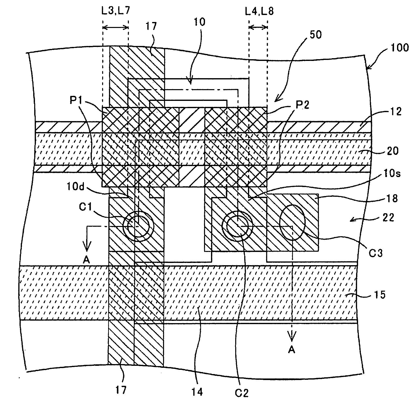
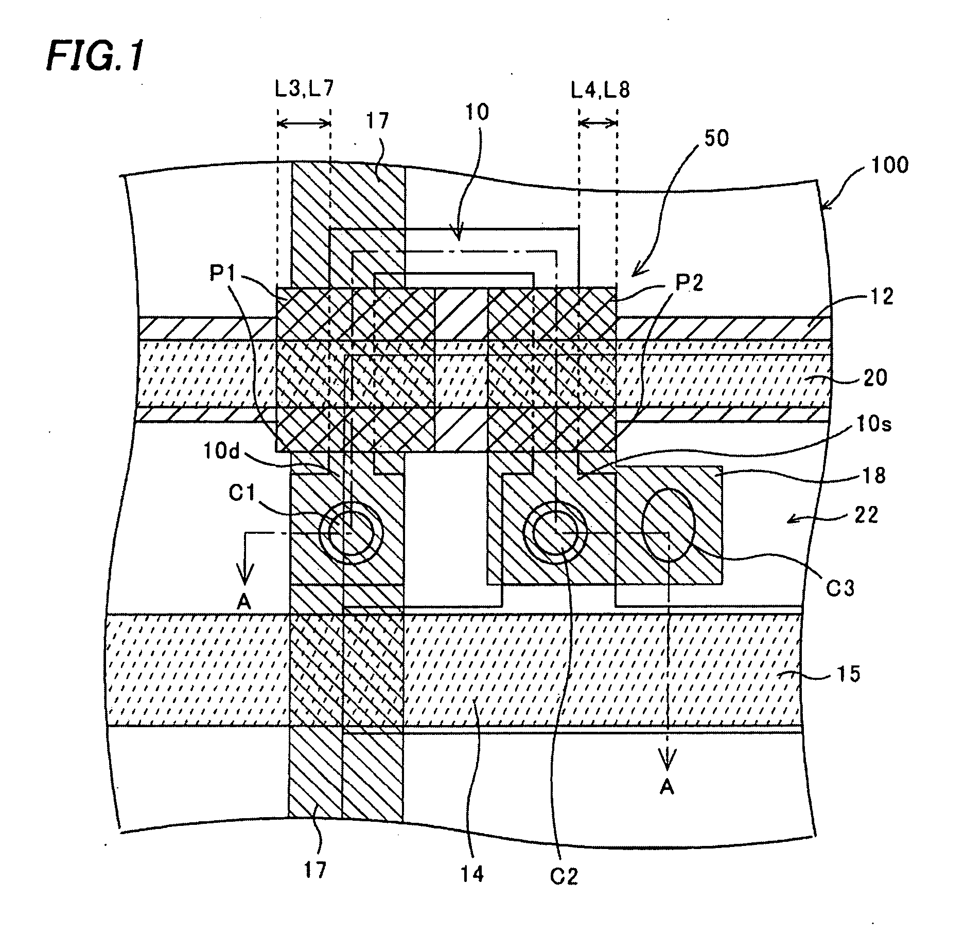
[0026] A liquid crystal display device of a first embodiment of the invention will be described referring to figures. This liquid crystal display device has a plurality of pixels arrayed in a matrix of n rows and m columns, like the display device shown in FIG. 14. A TFT of each of the pixels is shielded from light by a drain line and a source electrode on its upper side and by a light shield layer on its lower side, so that light entering from above or under the liquid crystal display device or this reflected light is prevented from entering a depletion layer of a semiconductor layer of the TFT that is a source of a leak current.

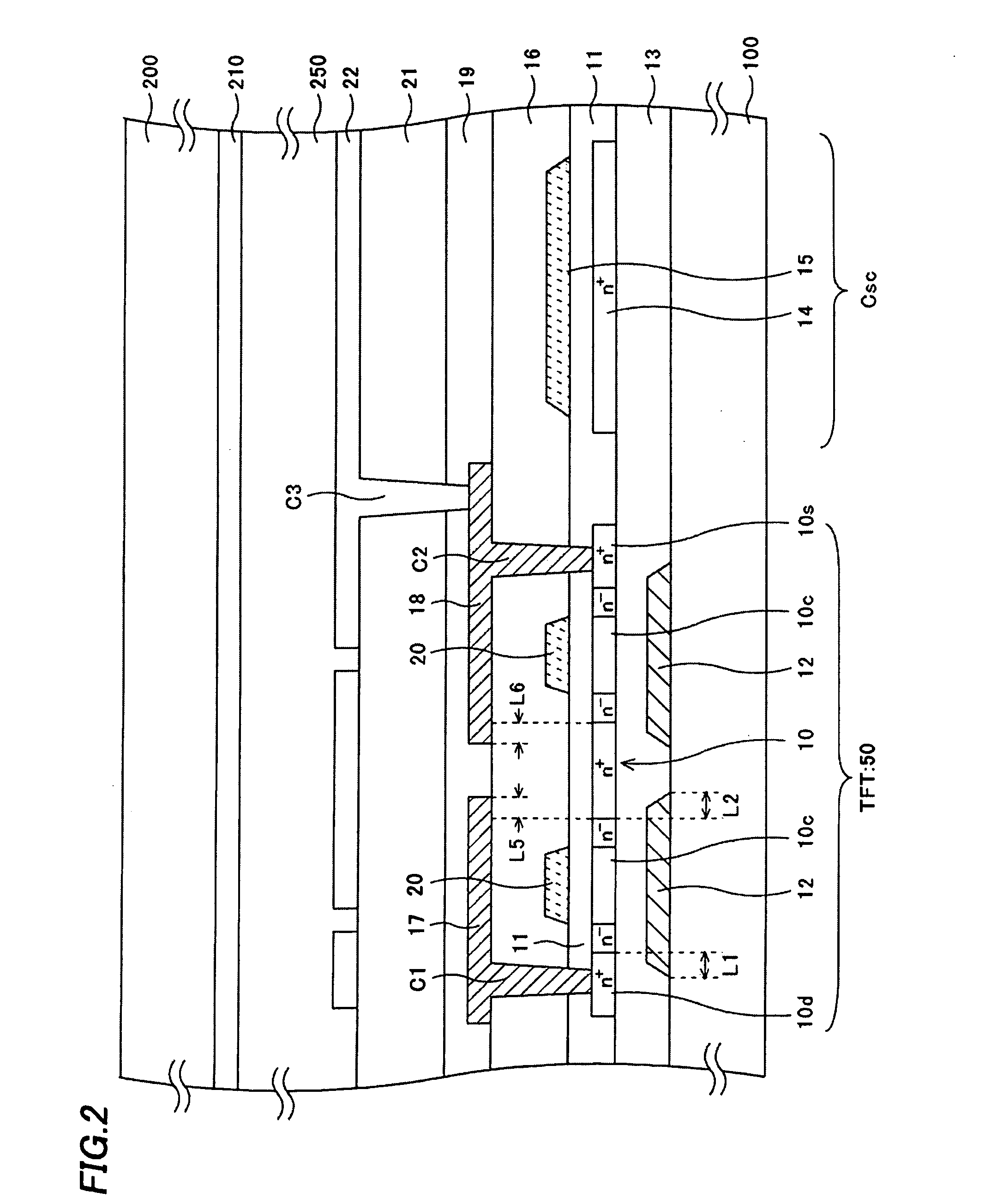
[0027]FIG. 1 is a plan view of a pixel of this liquid crystal display device, and FIG. 2 is a cross-sectional view of FIG. 1 along line A-A. A semiconductor layer 10 (e.g. made of a polysilicon layer) of a TFT 50 (that corresponds to a TFT 110 of FIG. 14) is formed on a first substrate 100 (e.g. a glass substrate) to have a pattern bending in a U-shape, an...


PUM

PropertyMeasurementUnit
thicknessaaaaaaaaaa
widthaaaaaaaaaa
widthaaaaaaaaaa

Abstract

The invention is directed to reduction of a leak current of a TFT of a pixel caused by light from a backlight or external light to improve a display quality of a liquid crystal display device. The display device of the invention includes a plurality of pixels on a first substrate, where each of the pixels includes a gate line intersecting a semiconductor layer with a gate insulation film interposed therebetween, a drain line connected to a drain region through a first contact hole and covering an upper side of the semiconductor layer extending from an intersection, and a source electrode connected to a source region through a second contact hole and covering an upper side of the semiconductor layer extending from an intersection. The device further includes a light shield layer formed under the semiconductor layer with a buffer film interposed therebetween and shielding the semiconductor layer from light.

Description

CROSS-REFERENCE OF THE INVENTION [0001] This application claims priority from Japanese Patent Application No. 2006-003484, the content of which is incorporated herein by reference in its entirety. BACKGROUND OF THE INVENTION [0002] 1. Field of the Invention [0003] The invention relates to a display device having a thin film transistor. [0004] 2. Description of the Related Art [0005] A conventional liquid crystal display device (referred to as LCD, hereafter) has a plurality of pixels arrayed in a matrix of n rows and m columns, and each of the pixels includes a pixel selection thin film transistor 10 (referred to as a TFT 110, hereafter), a liquid crystal LC, and a storage capacitor Csc, as shown in FIG. 14. It is noted that FIG. 14 shows only the pixels in two rows and two columns for simplification of the figure. [0006] A gate line 120 extending in the row direction is connected to a gate of the TFT 110, and a drain line 121 extending in the column direction is connected to a drai...

Claims


Application Information

Patent Timeline
Patent Type & Authority Applications(United States)
IPC IPC(8): G02F1/1343G02F1/1333
CPCG02F1/136209G02F1/136213G02F1/136227H01L27/1255H01L29/78621H01L29/78633H01L29/78696H01L29/41733
Inventor SEGAWA, YASUOONOGI, TOMOHIDE
Owner JAPAN DISPLAY WEST
Why Eureka
Try Eureka