Memory control apparatus and memory control method

a control apparatus and memory technology, applied in the field of memory control apparatus and memory control method, can solve problems such as devices that stop their operations, and achieve the effect of preventing data transfer and operating efficiently

Active Publication Date: 2007-07-26
MEGACHIPS
View PDF3 Cites 9 Cited by
  • Summary
  • Abstract
  • Description
  • Claims
  • Application Information

AI Technical Summary

Benefits of technology

[0026]Thus, an object of the present invention is to provide a technique for preventing data transfer from being restricted and allowing devices to operate efficiently, in an electronic apparatus in which data is transferred between a plurality of devices and a memory.

Problems solved by technology

Therefore, the buffers in the lower-priority devices may become completely empty of data or filled up with data, which may force the devices to stop their operations.

Method used


Image

  • Memory control apparatus and memory control method
  • Memory control apparatus and memory control method
  • Memory control apparatus and memory control method

Examples


Embodiment Construction

[0031]A preferred embodiment of the present invention will now be described referring to the drawings.

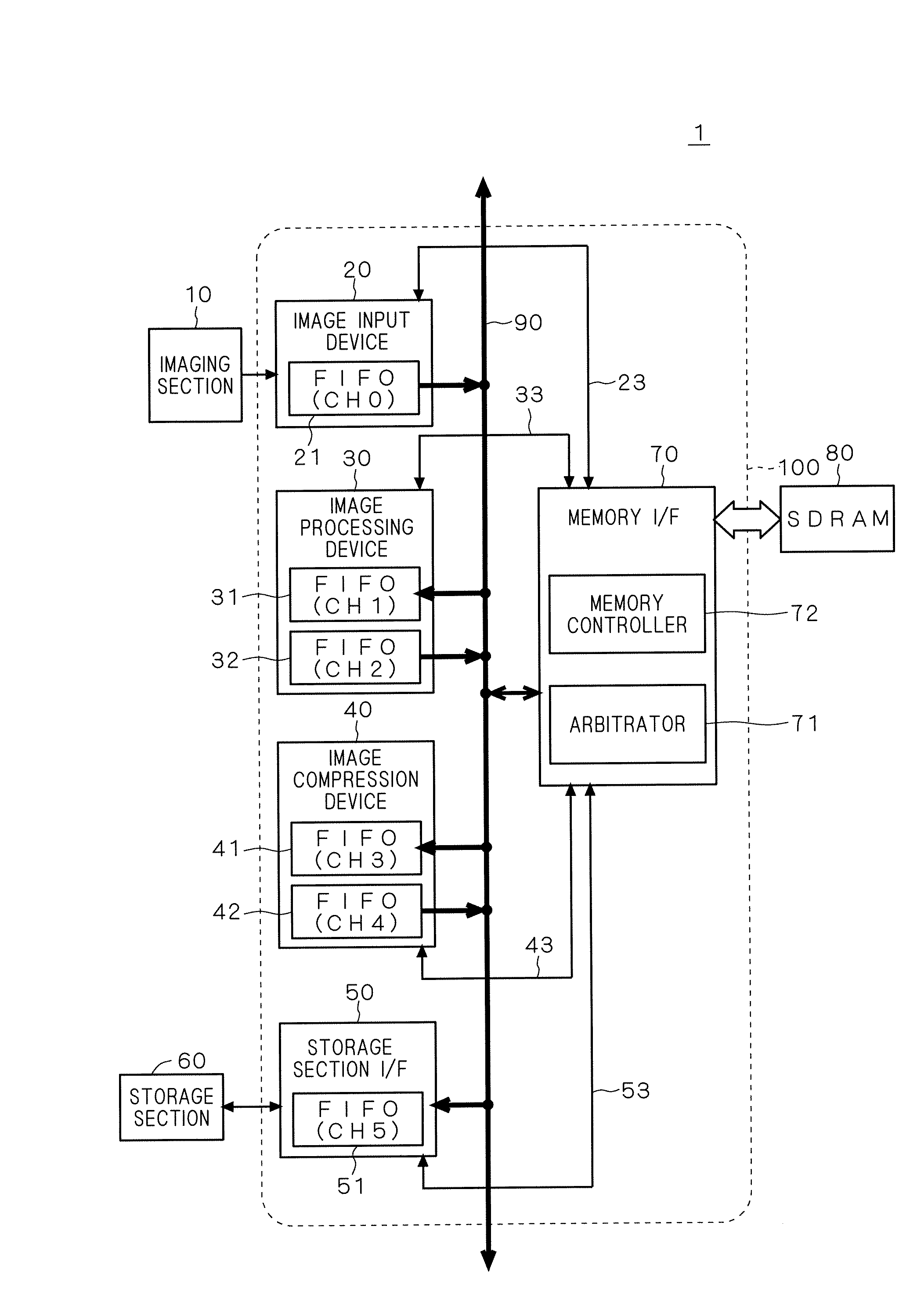
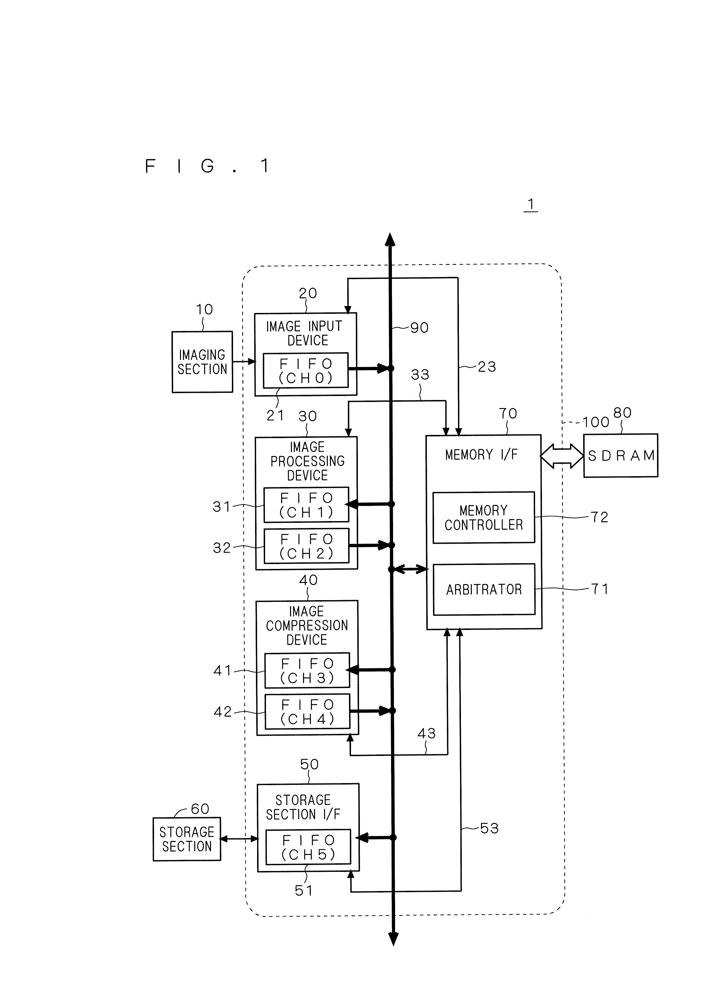
[0032]FIG. 1 is a block diagram illustrating the configuration of a digital still camera 1 that is equipped with a memory control apparatus of the present invention. The digital still camera 1 is an electronic apparatus that obtains image data, and it mainly includes an imaging section 10, an image input device 20, an image processing device 30, an image compression device 40, a storage section interface 50, a storage section 60, a memory interface 70, and an SDRAM 80. The image input device 20, the image processing device 30, the image compression device 40, and the storage section interface 50 are connected with the memory interface 70 through a data bus 90.

[0033]The imaging section 10 is a sensor that captures optical information from the object by converting the optical information to an electric signal. The imaging section 10 is formed of an imaging element such as a CCD or CMO...


PUM


Abstract

For an electronic apparatus in which data is transferred between a plurality of processing devices and a memory, a technique is provided which prevents the data transfer from being restricted and allows the processing devices to operate efficiently. The order of priorities of data transfer operations through channels is changed on the basis of a relation between thresholds and the amounts of data remaining respectively in FIFO buffers. This prevents the FIFO buffers from becoming empty of data, or from being filled up with data, which allows the devices to operate efficiently.

Description

BACKGROUND OF THE INVENTION[0001]1. Field of the Invention[0002]The present invention relates to a technique for transferring data between a plurality of devices and memory in an electronic apparatus.[0003]2. Description of the Background Art[0004]Electronic apparatuses, such as digital still cameras, are equipped with a plurality of processing units (devices) that apply various processes to image data and the like. The operation of such an electronic apparatus proceeds as these devices process data while sequentially transferring the data between memory and themselves.[0005]In such an electronic apparatus, each device is equipped with a buffer or buffers for temporarily storing the data transferred between the devices and memory. When data is transferred between a device and the memory, the data is once accumulated in a buffer of the device, and the accumulated data is sequentially sent to the destination. Data is thus transferred in succession without a break.[0006]However, in con...

Claims


Application Information

Patent Timeline
Patent Type & Authority Applications(United States)
IPC IPC(8): H04L12/56G06F12/00G06F13/362
CPCH04L47/10H04L47/30H04L47/29H04L47/2458
Inventor MATSUTANI, TAKASHI
Owner MEGACHIPS
Why Eureka
Try Eureka