Optical switching device, optical access network, optical switching method, program, and recording medium

a technology of optical switching and optical access network, which is applied in the direction of data switching network, multiplex communication, digital transmission, etc., can solve the problems of not always easy adjustment of nanosecond order, and achieve the effect of greatly extended transmission distance between an olt and an onu in the optical access network using the optical switching devi

Active Publication Date: 2007-07-26
NEC COMM SYST
View PDF5 Cites 26 Cited by
  • Summary
  • Abstract
  • Description
  • Claims
  • Application Information

AI Technical Summary

Benefits of technology

[0032] According to the present embodiments, the loss of about 4dB is reduced both in the downlink direction and in the uplink direction. Furthermore, the loss of the optical fiber between the OLT and the OSM vanishes since the optical signal from the center device side (OLT) is reproduced in the optical switching device (OSM). Therefore, the transmission distance between an OLT and an ONU in the optical access network using the optical switching device is greatly extended. Furthermore, the delay necessary before the downlink switch element is electrically achieved at high precision.

Problems solved by technology

However, the above-described conventional examples have the following problems.
Furthermore, the delay section 51 of FIG. 1 can be realized by adjusting the optical level, for example, the length of the optical fiber, but the delay section 51 requires adjustment of nanosecond order, which is not always easy.

Method used


Image

  • Optical switching device, optical access network, optical switching method, program, and recording medium
  • Optical switching device, optical access network, optical switching method, program, and recording medium
  • Optical switching device, optical access network, optical switching method, program, and recording medium

Examples


first embodiment

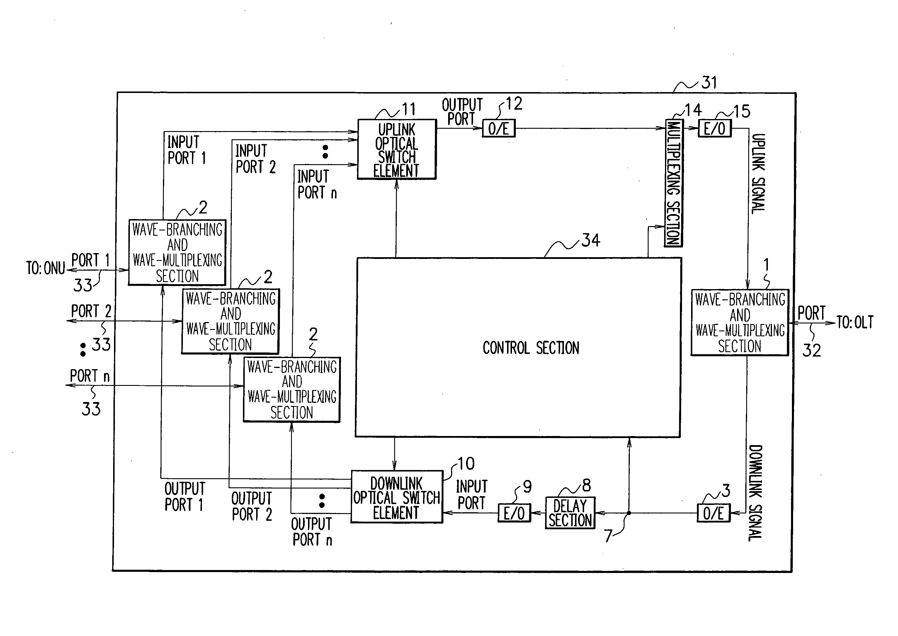
[0044] An optical switching device (OSM) according to a first embodiment will be described below with reference to FIG. 4.

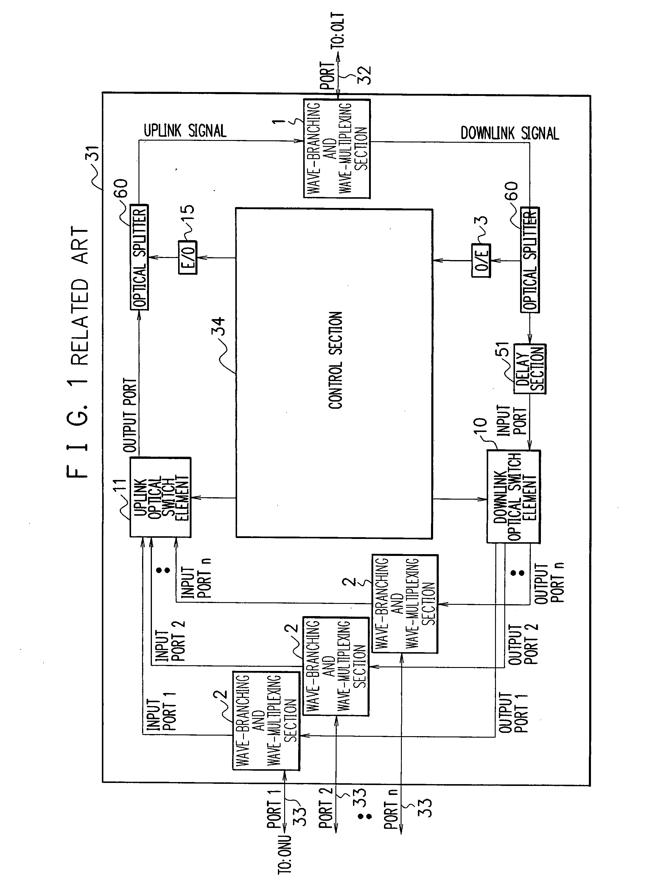
[0045] The optical switching device (OSM) 31 includes one input / output port connected to the OLT through an optical fiber 32 and n input / output ports connected to n ONUs through optical fibers 33. The input port of a downlink optical switch element 10 and the output port of an uplink optical switch element 11 in the OSM correspond to the port on the OLT side of the OSM 31. Output ports (=n) of the element 10 and n input ports of the element 11 in the OSM correspond to the ports on the ONU side of the OSM 31. The present embodiment has features that optical splitters for branching the optical signal is not included, the loss is small, and a delay section 8 is electrically achieved with high precision. When a CPU (Central Processing Unit) for performing a central processing control of the OSM 31 is used in the OSM 31, mounted are the CPU and ROM (Read Only Memory)...

second embodiment

[0058] An optical switching device (OSM) according to a second embodiment of the present invention will be described below with reference to FIG. 5.

[0059] The optical switching device (OSM) 31 includes one input / output port connected to an OLT through an optical fiber 32 and n input / output ports connected to n ONUs through optical fibers 33. An input port of a downlink optical switch element 10 and an output port of an uplink optical switch element 11 in the OSM correspond to the port on the OLT side of the OSM 31, and n output ports of the element 10 and n input ports of the element 11 in the OSM correspond to the ports on the ONU side of the OSM 31. The present embodiment has features that the downlink direction has a 3R function and the uplink direction has a 2R function, the round-trip time Tz between the OSM 31 and an ONU is acquired from an OLT, the optical splitter for branching the optical signal is not included, the loss is small, and a delay section 8 is electrically achi...

third embodiment

[0098] An optical switching device (OSM) according to a third embodiment of the present invention will be described below with reference to FIG. 6.

[0099] The optical switching device (OSM) 31 includes one input / output port connected to an OLT through an optical fiber 32 and n input / output ports connected to n ONUs through optical fibers 33. The input port of a downlink optical switch element 10 and the output port of an uplink optical switch element 11 in the OSM correspond to the port on the OLT side of the OSM 31, and n output ports of the downlink optical switch element and n input ports of the uplink optical switch element in the OSM correspond to the ports on the ONU side of the OSM 31. The present embodiment has features that the downlink direction and the uplink direction both have a 3R function, the round-trip time Tz between the OSM 31 and an ONU is obtained from the OLT, the optical splitter for branching the optical signal is not included, the loss is small, and a delay ...


PUM


Abstract

In an optical access network using an optical switching device, a 2×1 optical splitter in the uplink and downlink directions is eliminated to extend the transmission distance between the OLT and the ONU. An optical switching device includes a downlink optical switch element for switching a downlink optical signal sent by an OLT, an uplink optical switch element for switching an uplink optical signal sent by a plurality of ONU, an O / E for converting a downlink optical signal to a first electrical signal, an E / O for converting the first electrical signal to a downlink optical signal and inputting the downlink optical signal to the downlink optical element, an O / E for converting an uplink optical signal output from the uplink optical switch element to a second electrical signal, and an E / O for converting the second electrical signal to an uplink optical signal and sending the uplink optical signal to the OLT.

Description

BACKGROUND OF THE INVENTION [0001] 1. Field of the Invention [0002] The present invention relates to a configuration of an optical switching device used in an optical access network. The present invention relates to a technique that eliminates a 1×2 splitter, which has been needed in an optical switching device, and reduces insertion loss of the optical switching device. Further, the present invention relates to a technique that compensates the loss between an optical switching device (OSM (Optical Switching Module)) and a center device (OLT (Optical Line Unit)), and extends the transmission distance between the center device and a remote device (ONU (Optical Network Unit)). The present invention also relates to a technique that achieves with extremely high accuracy the delay, which is required for downlink switching, at an electrical level instead of the conventional optical level. [0003] 2. Description of the Related Art [0004] Japanese Patent Application Laid-Open No. 7-177098 (p...

Claims


Application Information

Patent Timeline
Patent Type & Authority Applications(United States)
IPC IPC(8): H04L12/56H04J14/00H04B10/27H04B10/00H04B10/272H04B10/291H04B10/556
CPCH04Q11/0066H04Q11/0071H04Q11/0067
Inventor NOMURA, TAKUMIUEDA, HIROMIMAKINO, KUNITETSUKUROKAWA, HIROAKITSUBOI, TOSHINORIKASAI, HIROYUKIKOBAYASHI, HIROKAZU
Owner NEC COMM SYST
Why Eureka
Try Eureka