Chemical filter unit

Inactive Publication Date: 2007-08-09
SAMSUNG ELECTRONICS CO LTD
View PDF4 Cites 8 Cited by
  • Summary
  • Abstract
  • Description
  • Claims
  • Application Information

AI Technical Summary

Benefits of technology

[0015]According to the present invention, a membrane that can collect particles is disposed inside the housing of a chemical filter unit. Also, a window, preferably in the form of a magnifying glass, allows the membrane to be viewed from outside the housing. Therefore, the degree to which the filter unit ha

Problems solved by technology

That is, a high quality semiconductor device can not be manufactured without the use of clean chemicals provided by one or more filters.
However, sometimes the chemicals used in a fabrication process become contaminated before the useful life of the filter unit expires.
In this case, the filter of the unit may fail to filter the chemicals sufficiently for s

Method used


Image

  • Chemical filter unit
  • Chemical filter unit
  • Chemical filter unit

Examples


Example

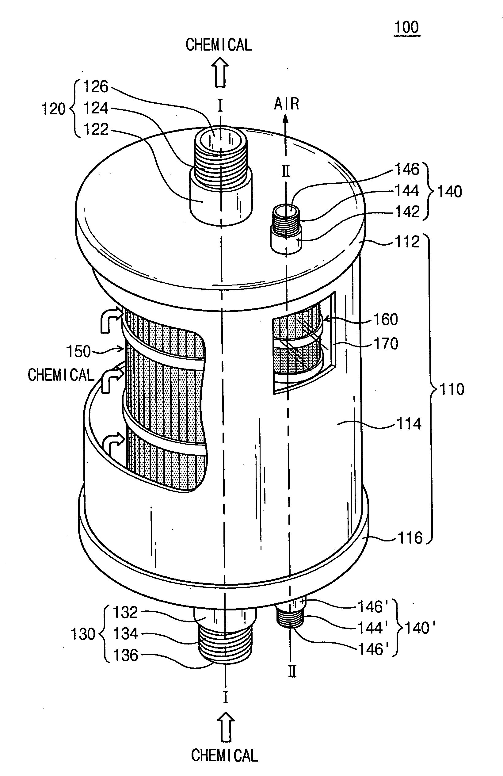
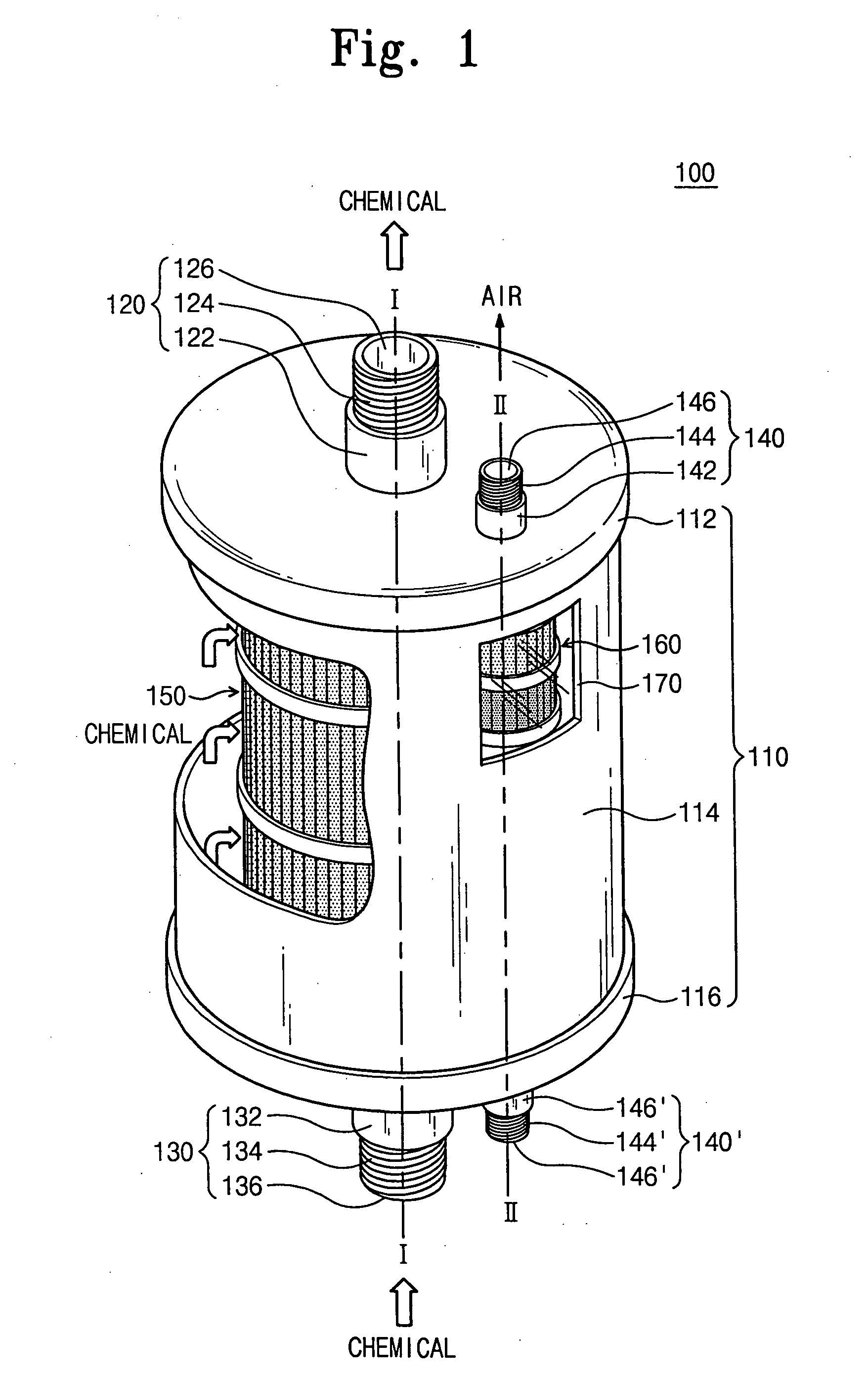
[0025]Referring to FIG. 1, an embodiment of a chemical filter unit 100 according to the present invention includes a housing 110 and a first filter 150 mounted within the housing 110. The housing 110 and the filter 150 each may be approximately cylindrical. The chemical filter unit 100 filters foreign substances or contaminants (referred to as “particles” hereinafter) from chemicals to purify the chemicals. An example of the chemicals that can be filtered by the chemical filter unit 100 is the photosensitive solution used in photolithography.

[0026]The housing 110 has a main body, and an inlet, an outlet and at least one air vent open to the interior of the main body. The first filter 150 is disposed in the main body of the housing in the path along which fluid flows from the inlet to the outlet. More specifically, the housing 110 has a cylindrical sidewall 114, and a top wall 112 and a bottom wall 116 coupled to the top and bottom of a cylindrical sidewall 114, respectively. The top...


PUM

PropertyMeasurementUnit
Sizeaaaaaaaaaa

Abstract

A chemical filter unit includes a housing, a first filter for filtering liquid chemicals, a second filter for filtering air, and a window in the housing. The housing has an outlet and an inlet through which chemicals enter and leave the filter, respectively, and an air vent that allows air to be discharged from the filter. The first filter is disposed in a path along which chemicals flow inside the housing to filter out particles contained in the chemicals, and the second filter is disposed in a path along which air leaves the filter through the air vent. The second filter includes a medium that collects particles contained in the air. The window allows the second filter to be seen from outside the housing.

Description

BACKGROUND OF THE INVENTION[0001]1. Field of the Invention[0002]The present invention relates to filters. More particularly, the present invention relates to filters for removing particles from chemical solutions used in the manufacturing of semiconductor devices and the like.[0003]2. Description of the Related Art[0004]Semiconductor devices must be manufactured under strict process conditions, using chemicals applied according to precise manufacturing techniques, and in an environment having a high level of cleanness. With respect to the latter, wafers from which the semiconductor devices are manufactured must be isolated during the manufacturing process from contaminants that would otherwise damage or adversely affect the characteristics of the resulting semiconductor device. One of the measures taken to prevent a wafer from being contaminated is to filter the chemicals used in semiconductor device manufacturing process. That is, a high quality semiconductor device can not be manu...

Claims


Application Information

Patent Timeline
IPC IPC(8): B01D53/22
CPCB01D29/21B01D36/001B01D46/24B01D46/4254B01D63/10B01D2313/44B01D63/14B01D71/32B01D29/52F24F13/28
Inventor BYUN, JU-SANGCHOI, KI-RYONG
Owner SAMSUNG ELECTRONICS CO LTD
Why Eureka
Try Eureka