Scanning electron microscope and apparatus for detecting defect

a scanning electron microscope and defect detection technology, applied in the field of electron microscope equipment, can solve problems such as the size of the defect of the fusion chamber, and achieve the effect of high contras

Active Publication Date: 2007-08-16
HITACHI HIGH-TECH CORP
View PDF4 Cites 14 Cited by
  • Summary
  • Abstract
  • Description
  • Claims
  • Application Information

AI Technical Summary

Benefits of technology

[0010] According to the present invention, an image of unevennesses may be obtained ...

Problems solved by technology

Recently, a finer production process for manufactu...

Method used


Image

  • Scanning electron microscope and apparatus for detecting defect
  • Scanning electron microscope and apparatus for detecting defect
  • Scanning electron microscope and apparatus for detecting defect

Examples


Embodiment Construction

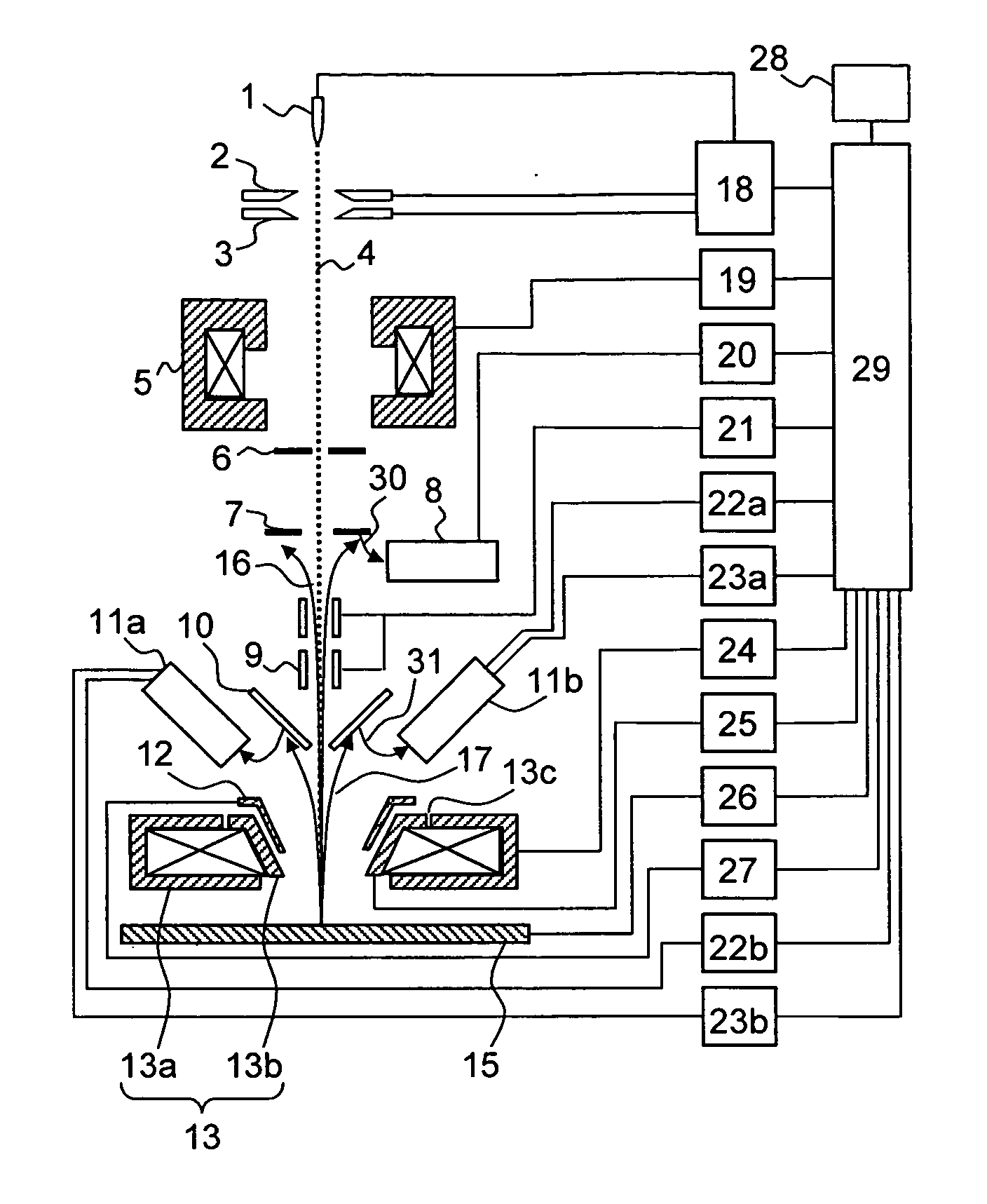
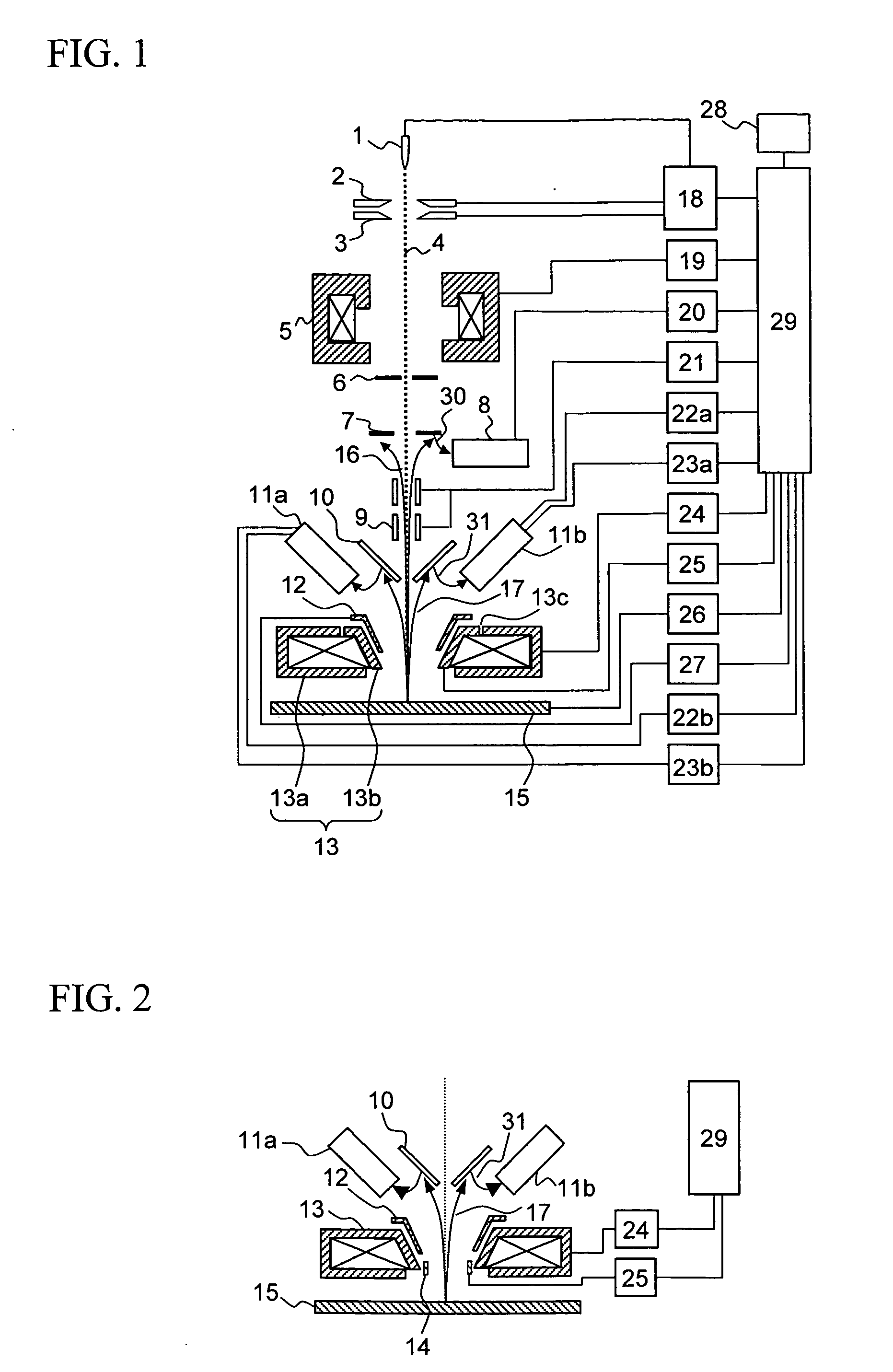
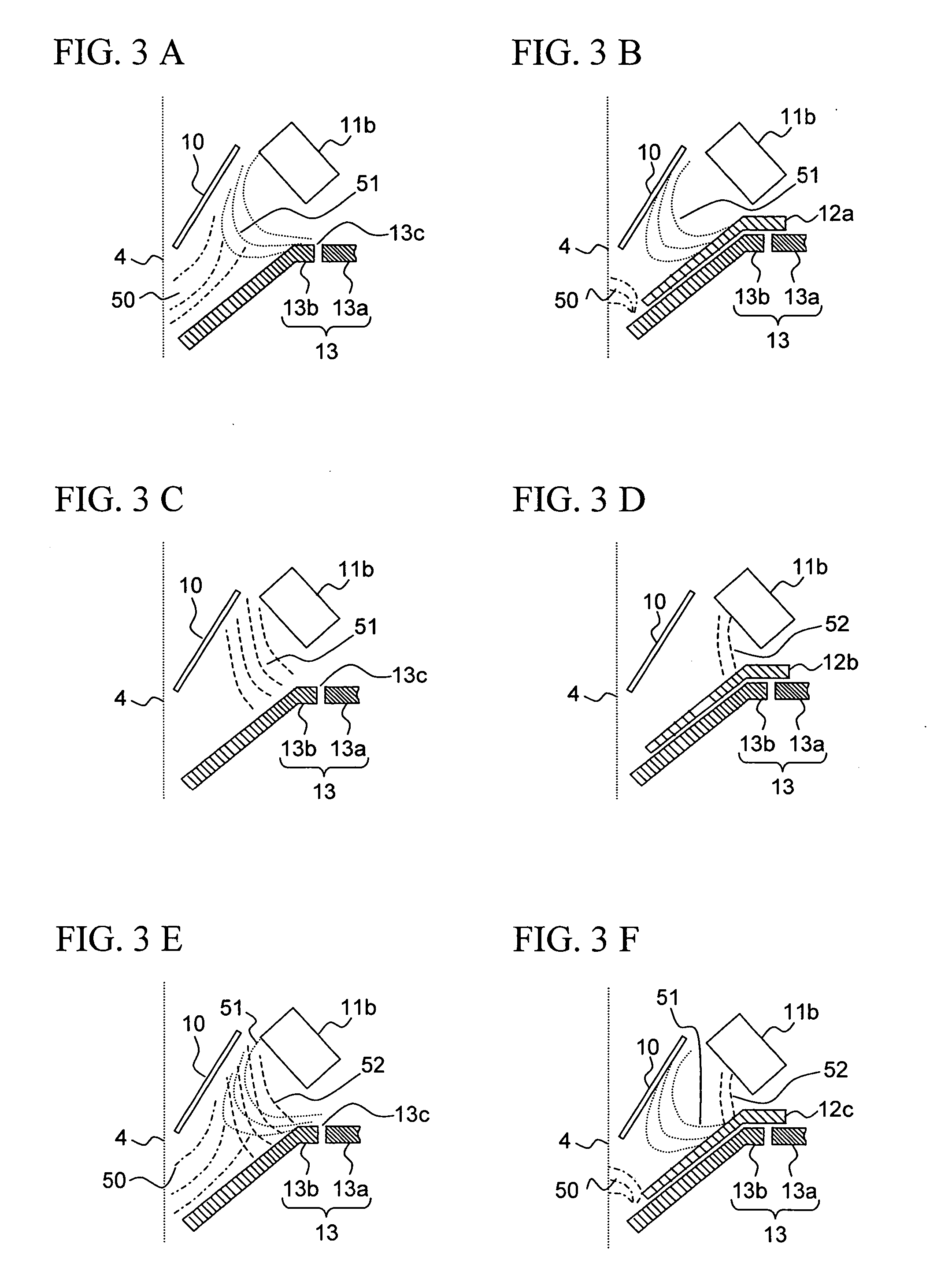
[0028]FIG. 1 shows one example of a scanning electron microscope according to the present invention. A scanning electron microscope according to the present example has a cathode 1, anodes 2 and 3, a focusing lens 5, a throttle plate 6, a first conductor plate 7, a first detector 8, a deflecting coil 9, a second conductor plate 10, second detectors 11a and 11b, a shielding plate 12, and an object lens 13. A sample 15 is arranged below the object lens 13. A scintillator may be used as an electron detecting unit in the second detectors 11a and 11b.

[0029] The scanning electron microscope according to the present example further has a high-voltage control power supply 18 which controls a high voltage applied to between the cathode 1 and the first and second anodes 2, 3; a focusing-lens control power supply 19 which controls a current passing through the focusing lens 5; a first amplifier 20 which amplifies a signal from the first detector 8; a deflecting-coil control section 21 which s...


PUM


Abstract

A scanning electron microscope, by which an image of unevennesses on the surface of a sample may be obtained in a high-resolution manner and a high contrast one, is provided according to the present invention. A sample image is obtained by use of the scanning electron microscope with a configuration in which a positive voltage is applied in order to accelerate a primary electron beam, and an electric field shielding plate, a magnetic field shielding plate, or an electromagnetic field shielding plate is arranged on the upper side of an object lens.

Description

BACKGROUND OF THE INVENTION [0001] 1. Field of the Invention [0002] The present invention relates to an electron microscope apparatus which is preferably used for detecting a defect in a wafer, and, more particularly, to a scanning electron microscope for image picking-up of unevennesses on the surface of a sample. [0003] 2. Description of the Related Art [0004] During processes for manufacturing a semiconductor device, there is executed in-line wafer inspection by which a defect in a wafer is inspected. The defect in the wafer is detected, and a reason for generation of the defect is located by analysis to realize yield improvement and stable operation of production lines. [0005] Conventionally, an optical apparatus for inspecting a defect had been used for inspecting a defect in a wafer, but, recently, there has been used an apparatus for inspecting a defect by use of a scanning electron microscope. The scanning electron microscope may obtain an image of fine unevennesses on the s...

Claims


Application Information

Patent Timeline
IPC IPC(8): G21K7/00H01J37/141H01J37/244H01J37/28
CPCH01J37/09H01J37/28H01J2237/2817H01J2237/12H01J2237/24592H01J2237/0262
Inventor TACHIBANA, ICHIROSATO, MITSUGUFUKADA, ATSUKOSUZUKI, NAOMASAFUKUDA, MUNEYUKI
Owner HITACHI HIGH-TECH CORP
Why Eureka
Try Eureka