Electronic component, semiconductor device, methods of manufacturing the same, circuit board, and electronic instrument

a technology of electronic components and semiconductor devices, applied in the direction of semiconductor devices, semiconductor/solid-state device details, electrical instruments, etc., can solve the problems of thermal stress, difficult quality control and handling of bare chips, etc., to achieve the effect of easy deformation, easy deformation, and easy absorbing of stress from the stress transmission portion

Inactive Publication Date: 2007-08-16
SEIKO EPSON CORP
View PDF26 Cites 27 Cited by
  • Summary
  • Abstract
  • Description
  • Claims
  • Application Information

AI Technical Summary

Benefits of technology

[0007] Since the semiconductor element and external electrode of the present invention are connected by the wiring, the pitch of external electrode can be converted as required. The stress transmission portion transmits stress from the external electrode to the stress relieving portion, and stress can be thus relieved.
[0072] In this way, when the supplementary transmission portion is formed, stress from the external electrode is transmitted to the stress relieving portion by means of the supplementary transmission portion, and a concentration of stress between the external electrode and the stress transmission portion can be prevented.

Problems solved by technology

However, quality control and handling of bare chips are difficult.
In such a CSP semiconductor device, an important problem is to relieve the thermal stress due to the differences in coefficient of thermal expansion between the semiconductor chip and the mounting board.

Method used


Image

  • Electronic component, semiconductor device, methods of manufacturing the same, circuit board, and electronic instrument
  • Electronic component, semiconductor device, methods of manufacturing the same, circuit board, and electronic instrument
  • Electronic component, semiconductor device, methods of manufacturing the same, circuit board, and electronic instrument

Examples


first embodiment

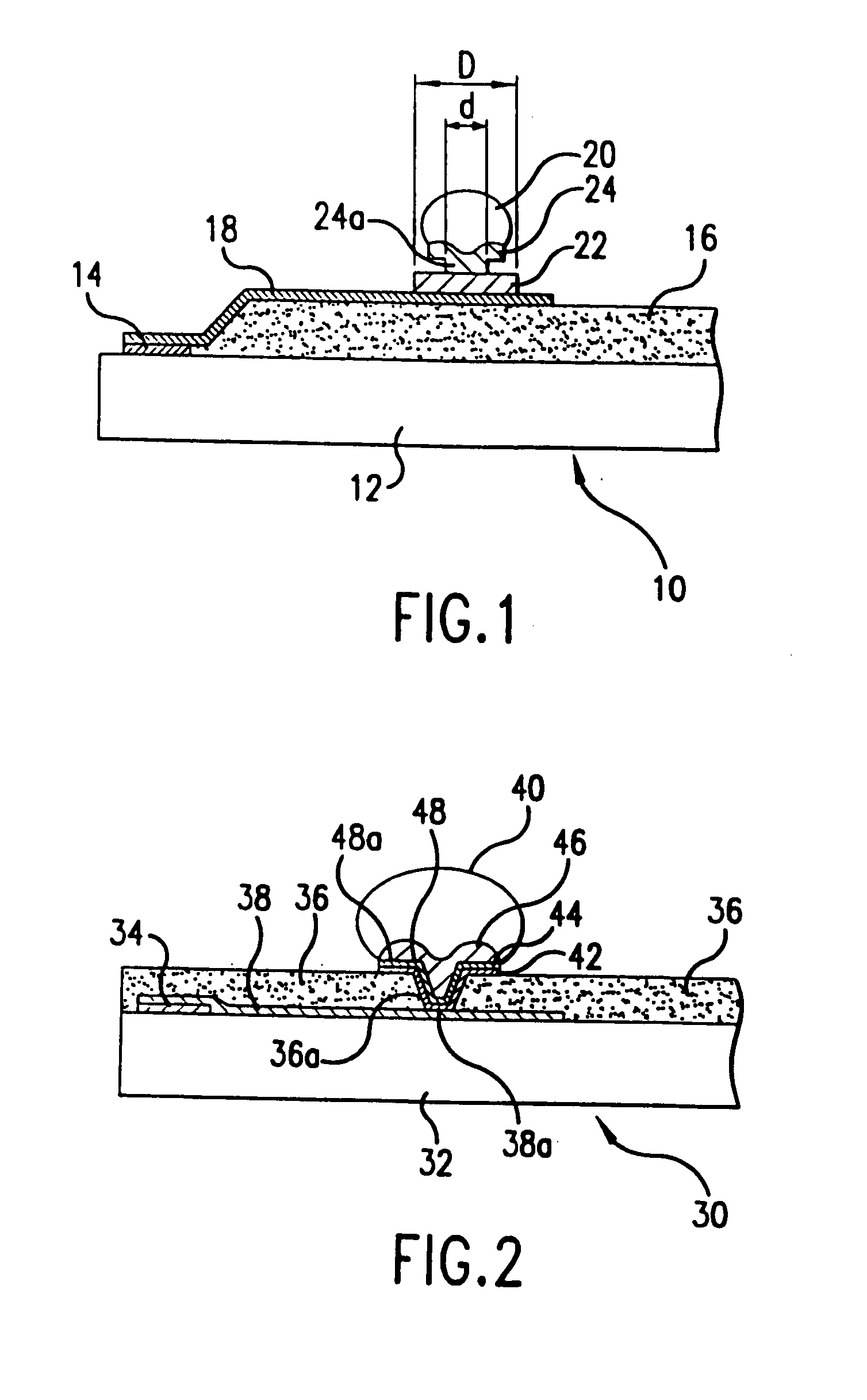
[0097]FIG. 1 is a sectional view showing a first embodiment of the semiconductor device. A semiconductor device 10 shown in this figure comprises a stress relieving layer 16 and wiring 18 formed thereon In more detail, on a semiconductor chip 12, a stress relieving layer 16 is formed to avoid an electrode 14, and wiring 18 is formed from the electrode 14 over the stress relieving layer 16.

[0098] The stress relieving layer 16 is formed from a photosensitive polyimide resin, and when the semiconductor device 10 is mounted on a substrate (not shown in the drawings), relieves the stress created by the difference in the coefficient of thermal expansion between the semiconductor chip 12 and the substrate. The polyimide resin is insulating with respect to the wiring 18, is able to protect the surface a and has heat resistance when a solder ball. 20 is melted. A polyimide resin with a low Young's modulus (such as an olefin polyimide resin or BCB manufactured by the Dow Chemical Corporation...

second embodiment

[0109]FIG. 2 is a sectional view showing a second embodiment of the semiconductor device. The semiconductor device 30 shown in this figure has wiring 38 formed beneath a stress relieving layer 36. In more-detail, on a semiconductor chip 32, with an oxide layer (not shown in the drawings) acting as an insulating layer interposed, wiring 38 is formed from an electrode 34. A stress relieving layer 36 is formed over this. It should be noted that the wiring 38 is formed of chromium (Cr).

[0110] In the stress relieving layer 36, a hole 36a is formed by photolithography, so that in the region of this hole 36a the wiring 38 is not covered by the stress relieving layer 36. In other words, the hole 36a is formed so that the wiring 38 is positioned directly under the hole 36a. Then a chromium (Cr) layer 42 and a copper (Cu) layer 44 are formed by sputtering applied to the wiring 38 and the inner circumferential surface and opening rim surface forming the hole 36a. In other words, the chromium ...

third embodiment

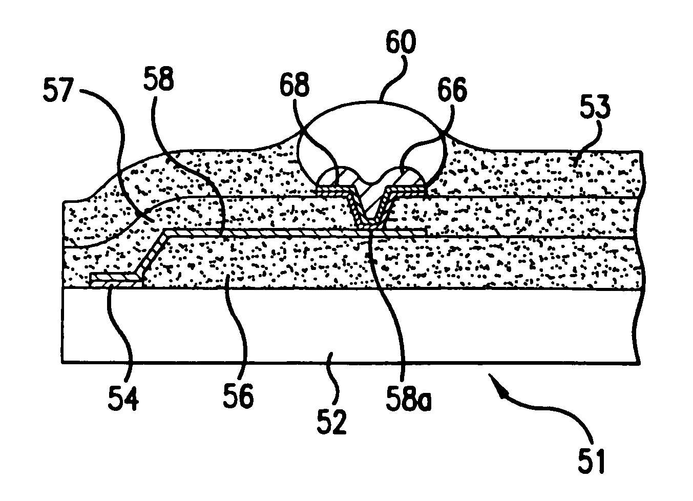
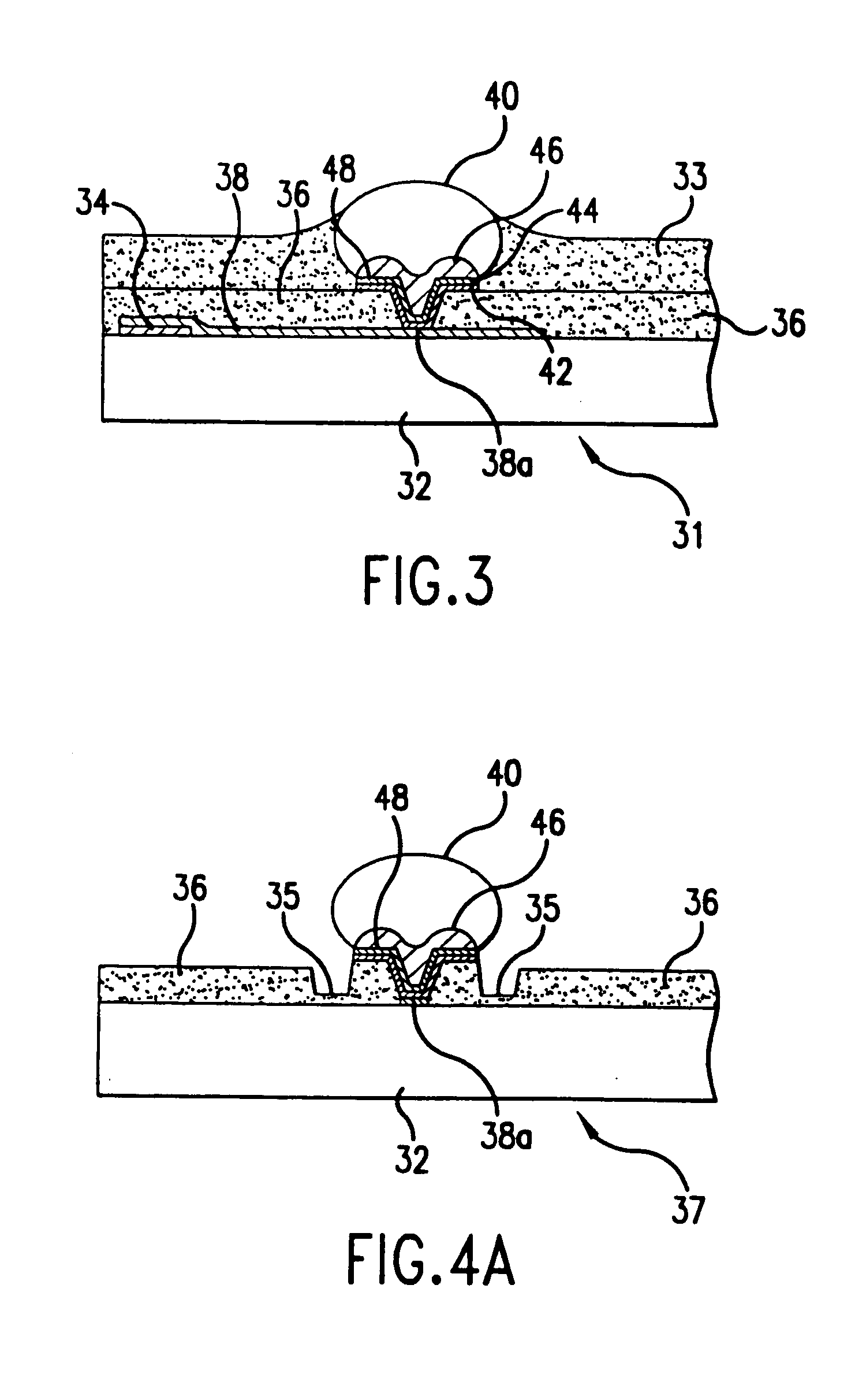
[0116]FIG. 3 is a sectional view showing a third embodiment of the semiconductor device. The semiconductor device 31 shown in this figure has a supplementary transmission layer 33 formed on the stress relieving layer 36 of the semiconductor device 30 shown in FIG. 2. In the present embodiment also, the connection portion 38a is a part of the chromium (Cr) layer 42, and is a part of the member electrically connecting the solder ball (external electrode) 40 and wiring 38.

[0117] The supplementary transmission layer 33 is formed in contact with, at least, the root periphery of the solder ball 40. Therefore, through the supplementary transmission layer 33, stress is transmitted from the solder ball 40 to the stress relieving layer 36. By this means, the stress is dispersed, and between the solder ball 40 and the stress transmission portion 48, in particular at the connecting portion of the base 46 with the copper (Cu) layer 44, a concentration of stress is avoided. It should be noted th...


PUM


Abstract

The present invention is a semiconductor device capable of relieving thermal stress without breaking wire. It comprises a semiconductor chip (12), a solder ball (20) for external connection, wiring (18) for electrically connecting the semiconductor chip (12) and the solder ball (20), a stress relieving layer (16) provided on the semiconductor chip (12), and a stress transmission portion (22) for transmitting stress from the solder ball (20) to the stress relieving layer (16) in a peripheral position of an electrical connection portion (24a) of the solder ball (20) and wiring (18).

Description

[0001] This is a Continuation of application Ser. No. 10 / 331,510 filed Dec. 31, 2002, which is a Continuation of application Ser. No. 09 / 953,858 filed Sep. 18, 2001, which is a Continuation of application Ser. No. 09 / 142,856 filed Mar. 26, 1999 which is a National Stage of PCT / JP98 / 00130 filed Jan. 16, 1998.TECHNICAL FIELD [0002] The present invention relates to a compact electronic component and a semiconductor device whose final formed package size is close to the size of the chip (semiconductor element), to methods of manufacturing these, to a circuit board on which these are mounted, and to an electronic instrument having this circuit board. BACKGROUND ART [0003] To pursue high density mounting in semiconductor devices, bare chip mounting is the ideal. However, quality control and handling of bare chips are difficult. For this reason, CSP (chip size / scale package) technology, in which the package size is close to the chip size, has been developed. [0004] In such a CSP semiconduc...

Claims


Application Information

Patent Timeline
Patent Type & Authority Applications(United States)
IPC IPC(8): H01L23/48H01L21/60H01L23/31H01L23/485
CPCH01L23/3114H01L2924/0002H01L24/05H01L24/11H01L2224/0231H01L2224/03912H01L2224/0401H01L2224/05599H01L2224/10126H01L2224/1132H01L2224/13022H01L2224/13023H01L2224/13099H01L2224/16H01L2924/01004H01L2924/01006H01L2924/01013H01L2924/01014H01L2924/01022H01L2924/01029H01L2924/01033H01L2924/01056H01L2924/01057H01L2924/01074H01L2924/01078H01L2924/01079H01L2924/01082H01L2924/014H01L2924/19041H01L2924/19043H01L24/13H01L2924/01024H01L2924/00014H01L24/03H01L2924/0001H01L23/3192H01L2224/131H01L2224/05572H01L2224/05558H01L2224/05556H01L2224/05018H01L2224/05027H01L2224/05552H01L2924/351H01L2924/12044H01L2224/0236H01L2924/00H01L23/12
Inventor HASHIMOTO, NOBUAKI
Owner SEIKO EPSON CORP
Why Eureka
Try Eureka