Unlock instant, AI-driven research and patent intelligence for your innovation.

Single poly non-volatile memory device with inversion diffusion regions and methods for operating the same

a non-volatile memory, single-poly technology, applied in the direction of semiconductor devices, basic electric elements, electrical apparatus, etc., can solve the problem of incompatibility of device b>100/b> with conventional cmos techniques, and achieve the effect of improving device density and overall siz

Active Publication Date: 2007-08-23
MACRONIX INT CO LTD
View PDF3 Cites 8 Cited by
  • Summary
  • Abstract
  • Description
  • Claims
  • Application Information

AI Technical Summary

Benefits of technology

[0014] In one aspect the assist gates are used to form inversion diffusion layers in the substrate. By using the assist gates to form inversion diffusion layers, the overall size of the device can be reduced, which can improve device density.

Problems solved by technology

This makes fabrication of device 100 incompatible with conventional CMOS techniques, which are single poly processes.

Method used


Image

  • Single poly non-volatile memory device with inversion diffusion regions and methods for operating the same
  • Single poly non-volatile memory device with inversion diffusion regions and methods for operating the same
  • Single poly non-volatile memory device with inversion diffusion regions and methods for operating the same

Examples


Embodiment Construction

.”

BRIEF DESCRIPTION OF THE DRAWINGS

[0017] Features, aspects, and embodiments of the inventions are described in conjunction with the attached drawings, in which:

[0018]FIG. 1 is a diagram illustrating a conventional floating gate memory device;

[0019]FIG. 2 is a diagram illustrating a conventional floating gate memory device that is compatible with the single poly fabrication process;

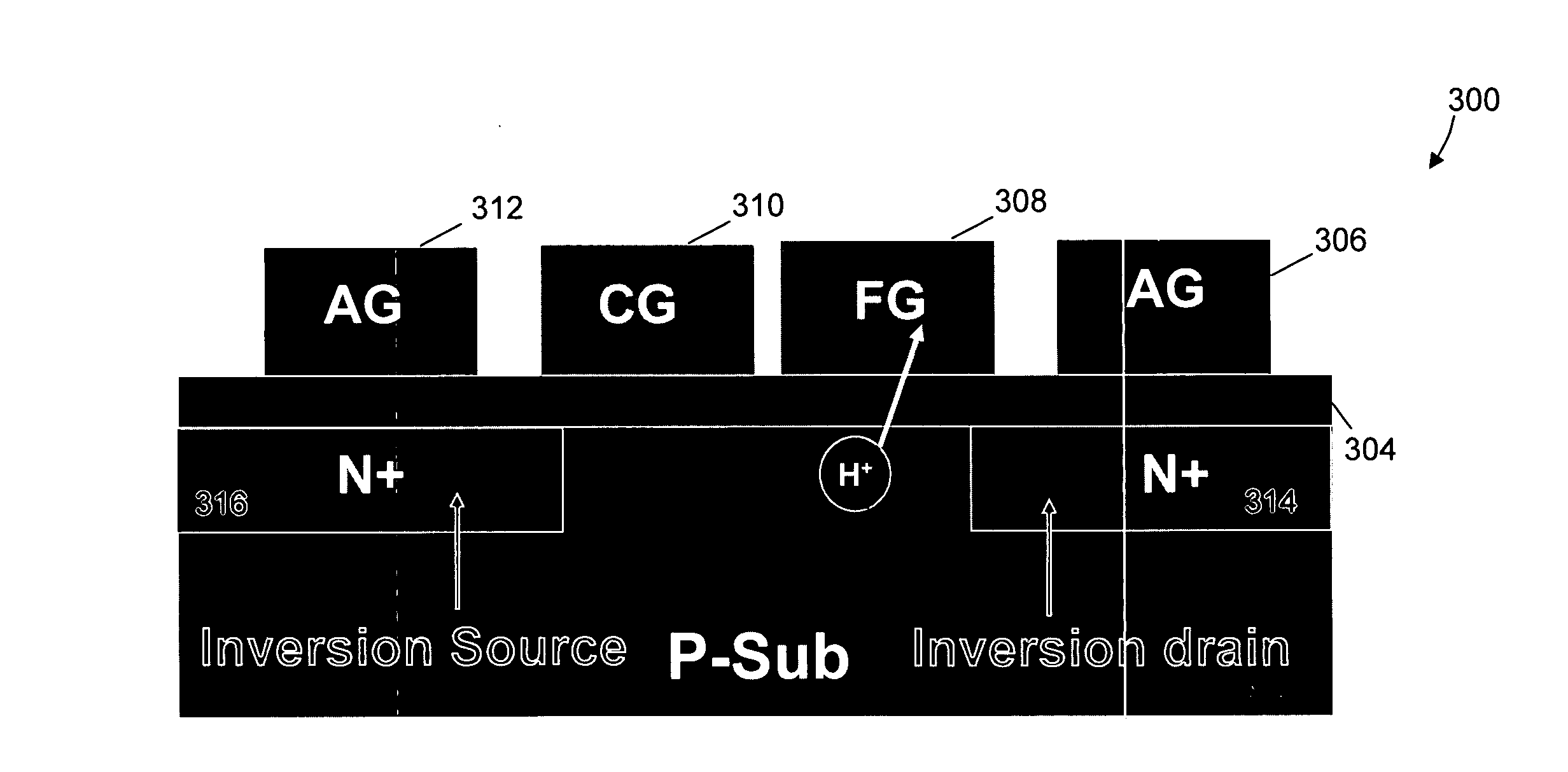
[0020]FIG. 3A is a diagram illustrating an NMOS non-volatile memory device configured in accordance with one embodiment;

[0021]FIG. 3B is a diagram illustrating a PMOS non-volatile memory device configured in accordance with another embodiment;

[0022]FIG. 4 is a diagram illustrating the coupling between a control gate and an assist gate with a floating gate for the device of FIG. 3A;

[0023]FIG. 5 is a diagram illustrating the dimensions associated with the gates and layers of the device in FIG. 3A;

[0024]FIG. 6 is a diagram illustrating an example of program operation for the device of 3A in accordanc...


PUM


Abstract

A non-volatile memory device comprises a substrate with the dielectric layer formed thereon. A control gate and a floating gate are then formed next to each other on top of the dielectric layer separated by a gap. Accordingly, a non-volatile memory device can be constructed using a single poly process that is compatible with conventional CMOS processes. In addition, assist gates are formed on the dielectric layer next to the control gate and floating gate respectively.

Description

BACKGROUND [0001] 1. Field of the Invention [0002] The embodiments described herein are directed to non-volatile memory devices, and more particularly to a non-volatile memory device comprising a single polysilicon gate layer that is compatible with CMOS processing techniques. [0003] 2. Background of the Invention [0004] Many non-volatile semiconductor memories are based on the well known MOS-type structure. In other words, they comprise a gate structure separated from a substrate by a dielectric layer. Diffusion regions are implanted in the substrate under the corners of the gate structure. When the appropriate voltages are applied to the diffusion regions and the control gate, a channel can be created in the upper layers of the substrate between the diffusion regions and under the gate structure. Carriers, e.g., electrons, can travel the channel between the diffusion regions. [0005] If a sufficient field component is present in the direction of the gate structure, the carriers, e....

Claims


Application Information

Patent Timeline
IPC IPC(8): H01L29/76
CPCH01L21/28273H01L29/42324H01L29/7883H01L29/66825H01L29/42328H01L29/40114
Inventor KUO, MING-CHANG
Owner MACRONIX INT CO LTD