Adaptive Design of Nanoscale Electronic Devices

a technology of electronic devices and nano-scale, applied in the direction of semiconductor/solid-state device testing/measurement, instruments, nuclear elements, etc., can solve the problems of difficult to fabricate nano-scale and other semiconductor devices that provide a desired transfer characteristic, the scaling of semiconductor devices such as transistors may eventually be limited by quantum effects, and the electron motion in the semiconductor device may be substantially limited

Active Publication Date: 2007-08-23
UNIV OF SOUTHERN CALIFORNIA
View PDF6 Cites 3 Cited by
  • Summary
  • Abstract
  • Description
  • Claims
  • Application Information

AI Technical Summary

Benefits of technology

[0006] A method of fabricating a semiconductor device so as to cause the device to have a desired transfer characteristic. Computations may be performed that predict a transfer characteristic of the semiconductor device for each of a plurality of different sets of values of available control parameters that may be used during the fabrication of the semiconductor device. A set of values of available control parameters that the computations predict will cause the semiconductor device to substantially provide the desired transfer characteristic may be identified, and the semiconductor device may be fabricated based on these identified values.

Problems solved by technology

The scaling of semiconductor devices, such as transistors, may eventually be limited by quantum effects.
This may make it difficult to fabricate nanoscale and other semiconductor devices that provide a desired transfer characteristic, such as one that is a particular polynomial function.
Electron motion in the semiconductor device may be substantially limited by quantum mechanical transmission.

Method used


Image

  • Adaptive Design of Nanoscale Electronic Devices
  • Adaptive Design of Nanoscale Electronic Devices
  • Adaptive Design of Nanoscale Electronic Devices

Examples


Embodiment Construction

[0032] Illustrative embodiments are now discussed. Other embodiments may be used in addition or instead. Details that may be apparent or unnecessary may be omitted to save space or for a more effective presentation.

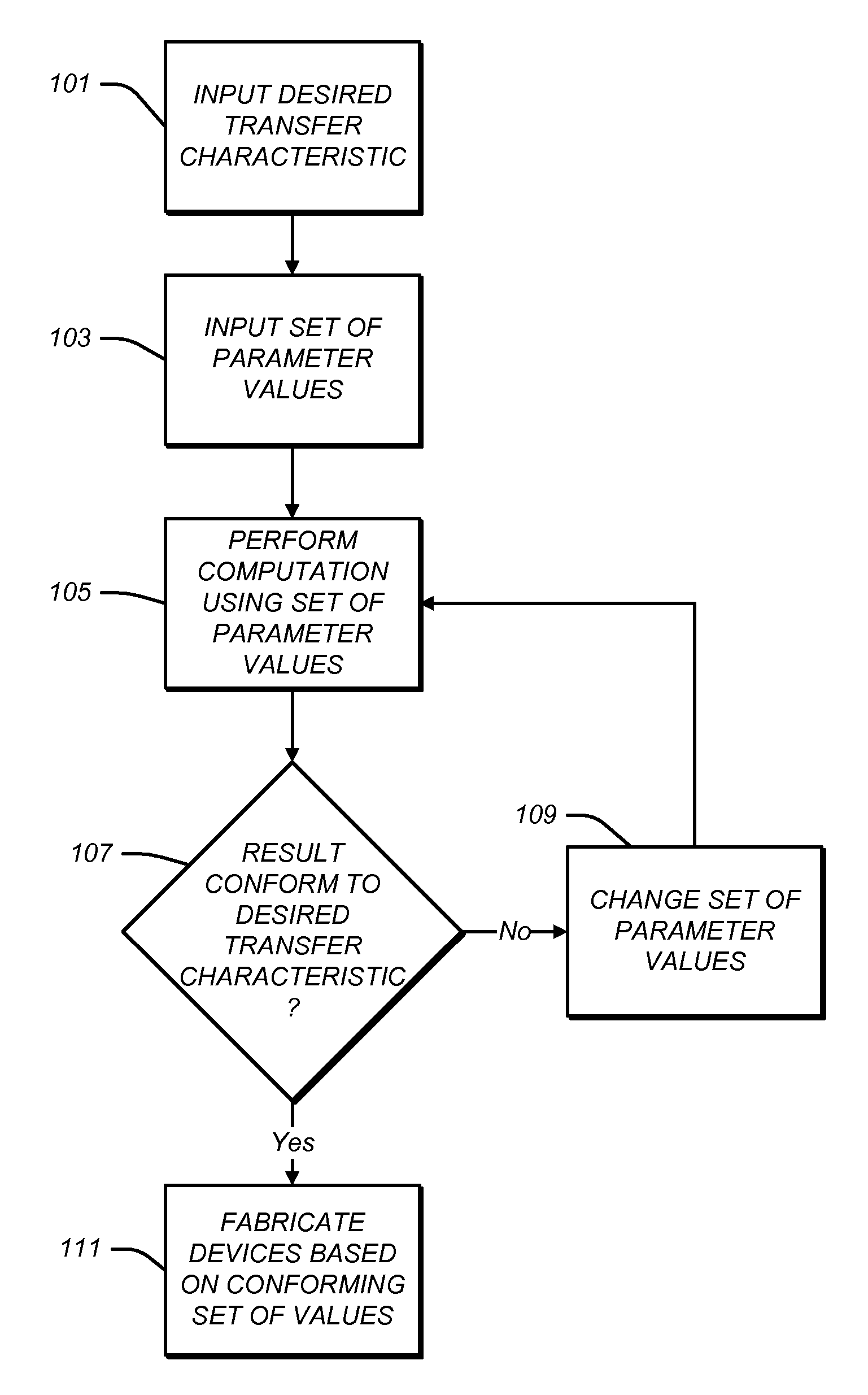
[0033]FIG. 1 illustrates a method for fabricating a semiconductor device.

[0034] A desired transfer characteristic of a semiconductor device to be fabricated may be inputted into a computational system, such as a computer system, as reflected by an Input Desired Transfer Characteristic step 101. The desired transfer characteristic may be of any type. For example, it may be an electron transmission voltage characteristic and / or a current voltage characteristic of the device. It may in addition or instead be a temporal response or frequency response. The characteristic may be for when electron motion in the semiconductor device is not at thermal equilibrium.

[0035] A set of control parameter values may next be inputted into the computational system, as reflected by an Inpu...


PUM


Abstract

A method of fabricating a semiconductor device so as to cause the device to have a desired transfer characteristic. Computations may be performed that predict a transfer characteristic of the semiconductor device for each of a plurality of different sets of values of available control parameters that may be used during the fabrication of the semiconductor device. A set of values of available control parameters that the computations predict will cause the semiconductor device to substantially provide the desired transfer characteristic may be identified, and the semiconductor device may be fabricated based on these identified values.

Description

CROSS-REFERENCE TO RELATED APPLICATION(S) [0001] This application is based upon and claims priority to U.S. Provisional Patent Application Ser. No. 60 / 776,073, entitled “Adaptive Design of Nanoscale Electronic Devices,” filed Feb. 23, 2006, attorney docket number 28080-198, the entire content of which is incorporated herein by reference.BACKGROUND [0002] 1. Field [0003] This disclosure relates to the fabrication of electronic devices, including semiconductor devices and nanoscale devices. [0004] 2. Description of Related Art [0005] The scaling of semiconductor devices, such as transistors, may eventually be limited by quantum effects. In this situation, semiconductor device dimensions may be a few nanometers. The resulting electric fields may be large enough to give rise to tunneling and non-equilibrium behavior that includes ballistic electron transport. This may make it difficult to fabricate nanoscale and other semiconductor devices that provide a desired transfer characteristic,...

Claims


Application Information

Patent Timeline
Patent Type & Authority Applications(United States)
IPC IPC(8): G06F17/50
CPCG06F17/505G06F30/327
Inventor LEVI, ANTHONY
Owner UNIV OF SOUTHERN CALIFORNIA
Why Eureka
Try Eureka